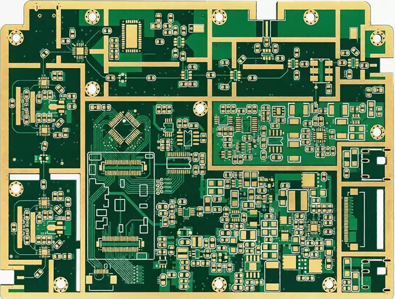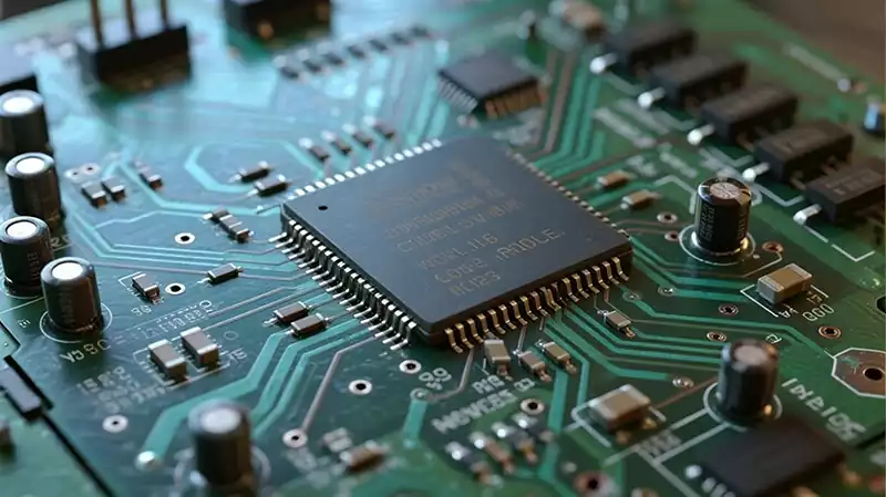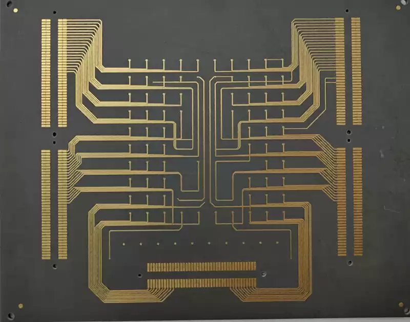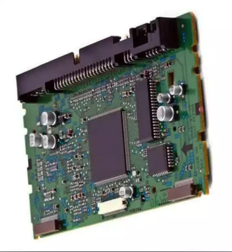
High-Speed Optical Module PCB: Core Challenges, Key Solutions, and Future Development Trends
The rapid evolution of global computing networks and 5G/6G communication infrastructure is accelerating the transition of optical module data rates from 400G to 800G and even 1.6T. Within this high-speed transmission ecosystem, the optical module PCB serves as the fundamental platform for optoelectronic signal transmission, component integration, and thermal management. As a result, it has […]