For high-frequency or high-speed digital circuits, wiring on FR4 materials is no longer as simple as just connecting components. Impedance-controlled design directly affects signal integrity, electromagnetic compatibility (EMC), and system stability. Centered around “how to optimize FR4 wiring through impedance control,” this guide provides engineers with actionable strategies and considerations during PCB design and manufacturing to achieve reliable and mass-producible high-speed board designs.
Essence and Objectives of Impedance Control
Essence: Impedance control involves maintaining the characteristic impedance of transmission lines (e.g., 50Ω, 75Ω, or differential 100Ω) within allowable tolerances on the PCB to minimize reflections and distortion during signal transmission.
Objectives: Reduce reflections, minimize crosstalk, improve rise/fall time retention, and enhance link jitter tolerance, thereby improving overall signal integrity and EMC performance.
Electrical Characteristics and Limitations of FR4 Materials
The relative permittivity (Dk) and loss tangent (Df) vary with frequency and board thickness. Manufacturing tolerances, glass fiber orientation, and resin content can affect actual impedance.
FR4 is suitable for applications from medium frequencies to several GHz, but stricter material selection and measurement calibration are required for millimeter-wave or high-precision differential pairs.
Key Parameters and Calculations During the Design Phase
Select Target Impedance: Confirm single-ended or differential target impedance and tolerance based on interfaces (e.g., SATA, USB, PCIe).
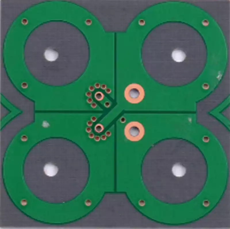
Transmission Line Types: Microstrip, stripline, and differential pairs; selection affects impedance calculation and EMC performance.
Geometric Parameters: Line width, spacing, layer spacing (dielectric thickness), and the position of interlayer reference planes (GND/POW).
Use Calculation Tools: Employ analytical formulas or simulations (2D field solutions/EM simulations) combined with real Dk/Df parameters for iterative design.
Common Optimization Strategies
Optimize Layer Stacking: Ensure high-speed signals have direct and continuous reference planes, preferring microstrip/stripline with adjacent ground layers; minimize reference plane switching.
Control Layer Spacing: Adjust dielectric thickness to achieve appropriate line widths, avoiding overly thin or wide lines that can cause manufacturing difficulties or crosstalk.
Differential Pair Routing: Maintain constant spacing, symmetrical routing, avoid unnecessary crossings and discontinuities; keep differential impedance consistent.
Avoid Sharp Corners and Sudden Changes: Use 45° or circular transitions; employ transition segments to buffer sudden changes in line width or layer spacing.
Crosstalk Management: Increase signal spacing, use ground return paths, and add blind/buried vias or ground plane isolation in critical areas.
Via Control: Reduce reflections and modal interference by adjusting via diameters, surrounding with ground blind/buried vias, or compensating impedance at vias (stitching, tented vias).
Matching and Termination: Use series/parallel impedance matchers or series termination resistors when necessary to reduce the return loss coefficient (S11).
Reference Plane Continuity: Minimize reference plane slots and maintain complete return paths through ground stitching vias.
Simulation Verification: Validate impedance spectra and crosstalk metrics using time-domain (TDR) or frequency-domain simulations before finalizing the PCB design.
Manufacturing and Process Considerations
Material Data Provision: Request actual measured Dk/Df and thickness tolerances from PCB suppliers, especially for target frequency bands.
Tolerance Setting: Clearly specify impedance targets and tolerances (e.g., 50Ω ±10% or differential 100Ω ±8%) in Gerber files and manufacturing instructions, and require impedance test reports from manufacturers.
Layering Process and Lamination: Pay attention to changes in dielectric thickness during lamination and assess the impact of blind/buried vias on interlayer thickness in advance.
Surface Treatment and Plating: Metal plating thickness (ENIG, HASL) affects impedance and manufacturing consistency and should be included in calculations.
Batch Consistency: Conduct statistical sampling inspections (TDR tests) on mass produced boards to ensure impedance remains within acceptable ranges for each batch.
Testing and Validation
TDR (Time-Domain Reflectometry) Testing: Validate single-ended and differential impedance distributions along the trace on prototypes and locate reflection sources.
S-Parameters and Eye Diagrams: Measure S-parameters, jitter, and eye diagram quality using network analyzers or vector oscilloscopes to assess link performance.
EMC Pre-Testing: Conduct early common-mode/differential-mode tests and adjust necessary filtering or grounding strategies.
By systematically implementing impedance control strategies throughout the design, simulation, manufacturing, and testing phases, FR4 boards can demonstrate reliable performance in high-speed applications. The key lies in early clarification of impedance targets, the use of accurate material parameters, optimization of layer stacking and routing details, and close collaboration with PCB manufacturers to ensure batch consistency.