In the realm of modern electronic hardware engineering, characterized by extremely high demands for surface heat management, soaring power densities, and harsh operating environments, traditional organic polymer substrates—such as FR-4 epoxy fiberglass boards, polyimide (PI) flexible boards, and aluminum-based copper-clad laminates (MCPCBs)—are gradually reaching their physical performance limits. Particularly in high-power LED lighting, automotive-grade inverters, 5G/6G RF front-ends, optical communication transceiver modules, aerospace, and power electronic modules (such as IGBT/SiC power semiconductors), high thermal conductivity, high insulation, low coefficient of thermal expansion, and excellent high-frequency dielectric properties have become rigid requirements for system-level design.
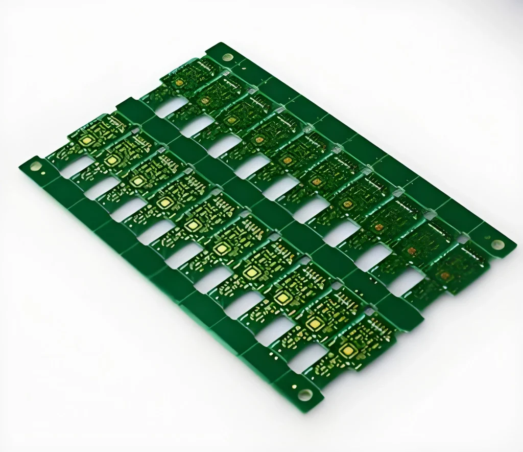
Against this backdrop, alumina circuit boards (typically referring to circuit boards made based on aluminum oxide (Al2O3) ceramic substrates) have become the absolute mainstay in the field of high-power and high-reliability electronic packaging due to their excellent comprehensive physical properties, extremely mature industrial supply chain, and superior cost-effectiveness.
A deep analysis of the materials science and physical mechanisms, microstructure characteristics, mainstream metallization manufacturing processes, thermal stress matching logic, high-frequency electromagnetic response, and engineering failure modes of alumina ceramic circuit boards is of significant engineering practical importance for building long-life, highly stable high-end hardware systems.
Materials Science and Microscopic Physical Properties of Alumina Ceramic Substrates
Alumina (Al₂O₃) is an inorganic non-metallic crystalline material with a mixture of strong ionic and covalent bonds. When used as a circuit board substrate, its performance is determined not only by the molecular structure of aluminum oxide (Al₂O₃) but also closely related to its purity, grain size, and sintering density.
Purity Classification and the Evolution of Physical Properties
In the electronics industry, the alumina ceramic substrate used to manufacture circuit boards is not pure single-crystal corundum but a polycrystalline ceramic produced through powder metallurgy sintering. Based on the percentage of aluminum oxide by mass, it is typically classified into three grades industrially:
96% Alumina Ceramic: This is currently the most widely used and cost-effective substrate specification in the electronics industry. It contains approximately 4% silicate glass phase sintering aids (such as silicon oxide, calcium oxide, magnesium oxide, etc.). The addition of sintering aids lowers the sintering temperature of the ceramic (typically between 1500°C and 1600°C), giving the substrate excellent physical rigidity and economy. Its thermal conductivity is typically between 24 and 28 W/m·K, approximately 80 times that of traditional FR-4 substrates.
99% and above high-purity alumina ceramics: Through fine powder preparation and ultra-high temperature sintering processes (above 1650°C), glass phase impurities are reduced to below 1%. High-purity alumina has a more compact grain, extremely low surface roughness, and thermal conductivity can be increased to 30 to 35 W/m·K. Due to the extremely low impurity content, its high-frequency dielectric loss is significantly reduced, and its breakdown voltage is greatly improved, making it commonly used in microwave RF thin-film circuits and demanding high-voltage insulation applications.
Toughened alumina ceramics (ZTA): A certain proportion of zirconium oxide (ZrO2) is doped into the alumina matrix. Utilizing the phase transformation toughening mechanism of zirconia under external impact, the physical defects of pure alumina ceramics—brittleness, low bending strength, and fragility—are greatly compensated for, resulting in a more than doubled mechanical fracture toughness. This makes it specifically designed for automotive-grade power modules subjected to severe mechanical vibration and high thermal shock.
Core Advantages in Thermal and Mechanical Properties
Compared to traditional organic and metal substrates, alumina ceramic circuit boards possess three irreplaceable physical properties: First, excellent thermal conductivity and high-temperature resistance. The alumina substrate has a melting point as high as 2050 degrees Celsius and exhibits extremely high thermal stability. Its thermal conductivity of over 25 W/m·K allows for rapid conduction and diffusion of heat generated by the chip’s heat source along the thickness direction, completely breaking through the “thermal resistance bottleneck” formed by traditional FR-4 insulating layers (with a thermal conductivity of only about 0.3 W/m·K).
Second, a coefficient of thermal expansion (CTE) that is highly compatible with silicon (Si), gallium nitride (GaN), and silicon carbide (SiC) chips. The coefficient of thermal expansion (CTE) of semiconductor silicon chips is approximately 3.5 to 4.0 x 10⁻⁶ Kelvin, while that of silicon carbide is approximately 4.5 x 10⁻⁶ Kelvin. In contrast, the CTE of alumina ceramics is approximately 6.5 to 7.5 x 10⁻⁶ Kelvin. This represents a significant physical mismatch between the CTE of traditional aluminum (approximately 23 x 10⁻⁶) and FR-4 (approximately 14 to 17 x 10⁻⁶) and that of the chip. When devices undergo severe thermal cycling, the alumina substrate minimizes thermal stress between the chip and the substrate, preventing fatigue cracking of solder joints due to thermal shear stress.
Thirdly, it exhibits extremely high volume resistivity and dielectric breakdown strength. Alumina itself is an excellent insulator, with a volume resistivity greater than 10¹⁴ ohm-cm and a breakdown voltage as high as 15 to 20 kV per millimeter. This means that high-voltage isolation of several kilovolts can be achieved on an extremely thin ceramic substrate without the need for an additional layer of easily aging insulating varnish.
Mainstream Metallization Manufacturing Processes for Alumina Ceramic Circuit Boards
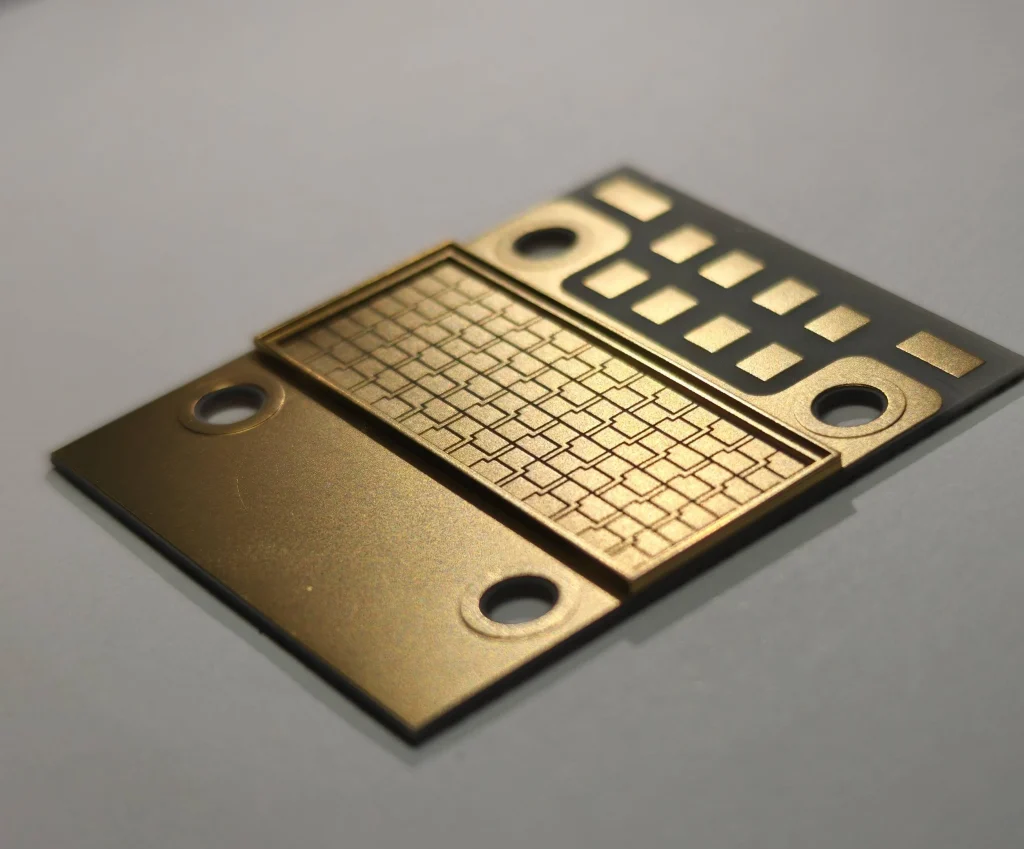
Alumina ceramic itself is an insulator. The core technology for manufacturing circuit boards from it lies in how to firmly deposit or bond a highly conductive and strongly adhesive copper (or gold, silver) layer onto its smooth, high-hardness ceramic surface. Based on different metallization mechanisms, the industry has currently developed four main technological routes:
Thick Film Technology (TFC) Thick film technology is the oldest and most mature method for manufacturing ceramic circuit boards.
The process involves using screen printing to print a viscous paste containing metal powder (such as silver-palladium alloy, gold, copper), glass powder particles, and an organic carrier onto an alumina ceramic substrate. After drying, the substrate is placed in a tunnel furnace for high-temperature sintering at 800 to 900 degrees Celsius in air or a reducing atmosphere. During sintering, organic matter completely volatilizes, and the molten glass powder liquid phase wets the alumina surface. After cooling, it tightly anchors the metal particles onto the ceramic substrate, forming conductive circuits.
Technical Features: Simple process, low equipment investment, extremely suitable for mass production, and excellent high-temperature resistance.
Engineering Limitations: Due to limitations in screen printing mesh and paste rheology, the minimum linewidth/space of thick-film circuits is typically difficult to achieve below 100 micrometers. Furthermore, the thick film layer contains some porosity, with a conductivity approximately 60% to 80% of pure copper, and the film thickness is relatively thin (typically 10 to 20 micrometers), making it difficult to withstand large currents in the hundreds of amperes.
Thin Film Technology / DPC – Direct Plated Copper: Direct plated copper technology (DPC) is a mainstream technology for achieving high-precision wiring on alumina ceramics using semiconductor manufacturing processes.
The process flow is as follows: First, the alumina ceramic surface undergoes ultrasonic cleaning and plasma etching activation. Then, in a cleanroom, a layer of titanium (Ti) or chromium (Cr) tens of nanometers thick is deposited on the ceramic surface as a seed/binder layer using physical vapor deposition (PVD) vacuum sputtering (because titanium/chromium has a strong chemical affinity for oxygen atoms in alumina). Subsequently, a copper seed layer is sputtered onto the titanium layer. Next, photoresist is coated, exposed through a mask, and developed to reveal the circuit pattern. Finally, a thickened copper layer is electroplated (the thickness can be controlled from several micrometers to hundreds of micrometers), the photoresist is stripped, and excess titanium-copper seed layer is removed by micro-etching.
Technical Features: Extremely high circuit precision, with linewidth and spacing down to below 10 micrometers, making it ideal for high-density packaging; excellent surface flatness, allowing direct wire bonding; and extremely high adhesion.
Engineering Limitations: Extremely expensive equipment investment, demanding production environment requirements, and difficulty in achieving copper layer thicknesses of several hundred micrometers or more, resulting in high costs for extremely thick copper electroplating.
Direct Bonded Copper (DCB) technology is the most widely used manufacturing process for ultra-high current ceramic substrates in power electronics (such as IGBT modules). Its physical mechanism is based on the formation of a copper-oxygen eutectic liquid between 1065°C and 1083°C. At this high temperature, the molten eutectic liquid phase simultaneously wets both the copper foil and the alumina ceramic surface. Upon cooling, it forms an extremely hard copper-alumina (CuAlO2) spinel mesophase, firmly “fusing” the thick copper foil (typically 100 to 800 micrometers thick) to both sides of the alumina substrate.
Technical characteristics: Extremely thick copper layer (up to 0.8 mm or more), with extremely high current carrying capacity and extremely low thermal resistance; excellent insulation withstand voltage performance; good thermal cycling stability.
Engineering limitations: High-temperature bonding processes easily generate micropores at the interface; severe lateral corrosion during thick copper etching limits the linewidth and spacing (typically requiring 0.3 mm or more); and the significant difference in thermal expansion coefficients between the ceramic and thick copper can easily cause the ceramic plate to crack under extreme temperatures.
Active Metal Brazing (AMB) Technology: AMB technology is a significant upgrade from DBC technology, representing the highest level of current ceramic metallization technology.
The process involves printing a layer of solder paste containing active metal elements such as titanium (Ti), zirconium (Zr), and a silver-copper alloy between alumina (or silicon nitride, aluminum nitride) ceramic and copper foil, followed by high-temperature brazing at approximately 800 degrees Celsius in a vacuum furnace. The active titanium metal reacts strongly with the oxides on the ceramic surface at high temperatures, generating a conductive metallization reaction layer, thereby bonding the thick copper foil to the ceramic with extreme firmness.
Technical Features: Significantly higher bonding strength than DBC; orders-of-magnitude improvement in thermal shock resistance and thermal cycling life, easily withstanding thousands of severe thermal cycles from -55°C to 175°C; and particularly suitable for use with toughened alumina (ZTA).
Engineering Limitations: Activated metal solder paste is extremely expensive, vacuum soldering is complex, and subsequent chemical etching to remove residual active metal layers is extremely difficult.
Thermal Physics Management and Thermal Stress Buffering Mechanisms
In power semiconductor packaging, alumina ceramic circuit boards are not only electrical connection carriers but also “thermal lenses” and “stress buffers” for the entire system.
Microscopic Conduction Model of Real Thermal Resistance
When evaluating the heat dissipation capacity of a circuit board, it is essential not only to consider the thermal conductivity of the substrate but also to analyze the total system thermal resistance from the chip junction to the heatsink.
The total system thermal resistance can be considered as a series combination of multiple interfacial thermal resistances and bulk material thermal resistances. The poor heat dissipation of traditional FR-4 substrates is due to the strong scattering of phonons (microscopic quantum carriers of heat transfer in solid materials) by the internal epoxy resin molecular network.
In contrast, in alumina ceramic circuit boards, heat is primarily transferred at high speed through a flow of phonons generated by lattice vibrations. Although the thermal conductivity of alumina (25 W/m·K) is lower than that of aluminum nitride (approximately 170 W/m·K) and silicon nitride (approximately 80 W/m·K), alumina boards can achieve exceptionally good heat spreading through a well-designed DBC or AMB thick copper structure. The thick top copper foil first rapidly diffuses heat from the concentrated heat source beneath the chip horizontally, greatly increasing the heat-receiving area. Then, the heat is vertically conducted to the large-area copper foil underneath through a thin alumina ceramic layer (e.g., 0.38 mm or 0.635 mm), significantly reducing the overall thermal resistance of the system.
Coefficient of Thermal Expansion (CTE) Matching and Shear Stress Relief
In power electronic modules, the coefficient of thermal expansion (CTE) of copper is approximately 16.5 x 10⁻⁶ Kelvin, while that of silicon is approximately 3.5 x 10⁻⁶ Kelvin. If a silicon chip is directly soldered onto a copper plate, the expansion of copper is far greater than that of silicon when the device heats up during operation. This generates enormous physical shear stress in the solder layer at the bottom of the chip. Repeated thermal expansion and contraction lead to microscopic grain boundary sliding and void expansion in the solder layer, ultimately resulting in solder detachment and chip burnout.
With the introduction of alumina ceramic circuit boards, alumina (CTE approximately 6.8) falls between that of silicon and copper.
When using a double-sided copper-clad DBC or AMB structure, the upper copper foil, the middle ceramic layer, and the bottom copper foil form a symmetrical “sandwich” structure. The strong rigidity of the ceramic layer greatly constrains the thermal expansion behavior of the thick copper foil on both sides, forcibly reducing the apparent thermal expansion coefficient of the entire alumina ceramic circuit board to around 7.0 to 8.5, achieving a high degree of matching with silicon and silicon carbide chips. This is equivalent to establishing a “thermal stress buffer” between the rigid chip and the high-expansion metal, reducing fatigue stress at the solder joint by more than 80%, and greatly extending the module’s lifespan.
High-Frequency Electromagnetic Response and Microwave Transmission Line Performance
In 5G/6G millimeter-wave communication, satellite receivers, and high-frequency radar systems, alumina ceramic circuit boards have become the preferred carrier for microwave integrated circuits (MMICs) and thin-film microstrip circuits due to their excellent high-frequency electromagnetic properties.
High-Frequency Stability of Dielectric Constant (Dk) and Dielectric Loss Tangent (Df)
In the microwave band, the dielectric properties of the circuit board substrate directly determine the propagation speed and energy attenuation of electromagnetic waves in the transmission line. Relative permittivity (Dk): The permittivity of 96% alumina ceramics is approximately 9.3 to 9.5, while that of high-purity 99.9% alumina is approximately 9.8 to 10.1. A higher permittivity means that the physical size of the circuit can be effectively reduced when transmitting electromagnetic signals of the same wavelength (the wavelength of the signal in the medium is inversely proportional to the square root of the permittivity), which is extremely advantageous for miniaturized RF front-end modules. More importantly, the permittivity of alumina maintains an almost flat curve across an extremely wide frequency band from megahertz (MHz) to hundreds of gigahertz (GHz), without significant dielectric dispersion with frequency. Dielectric loss tangent (D_f): At high frequencies of 10 GHz, the dielectric loss tangent of high-purity alumina ceramics is as low as 0.0001 to 0.0003 (while ordinary FR-4 is around 0.02, and high-performance Rogers PTFE sheets are around 0.001). Extremely low dielectric loss means that when microwave signals propagate along ceramic transmission lines, very little electromagnetic energy is converted into heat and dissipated, ensuring the phase consistency of high-frequency signals and extremely low insertion loss.
Surface Roughness and the Skin Effect: Under high-frequency alternating current, the current is no longer uniformly distributed across the entire cross-section of the conductor, but instead concentrates within a thin layer on the conductor’s surface. This physical phenomenon is called the skin effect. The skin depth decreases sharply with increasing frequency. For example, at 10 GHz, the skin depth of a copper conductor is only about 0.66 micrometers. If the surface of the ceramic substrate is extremely rough, the interface of the physically plated or sputtered copper layer will also exhibit an uneven morphology. When the skin depth is less than or equal to the surface roughness, the high-frequency current will be forced to flow tortuously along the uneven metal interface, resulting in a significantly longer effective physical path for the conductor, which in turn leads to huge high-frequency conductor losses and signal phase distortion. High-purity alumina ceramic circuit boards prepared using thin-film DPC technology can have their surface roughness (Ra) precisely controlled to below 0.05 micrometers (achieving mirror-like finish) through precision polishing. This extremely smooth interface allows for smooth and unimpeded transmission of high-frequency skin current, greatly suppressing skin effect losses at high frequencies. This is a key physical guarantee for millimeter-wave circuits to achieve extremely low noise transmission.
Assembly, Soldering, and Bonding Processes and Engineering Failure Mode Analysis
Despite the numerous physical advantages of alumina ceramic circuit boards, their inherent brittleness and the special characteristics of inorganic materials necessitate strict adherence to engineering specifications during surface mount assembly, wire bonding, and actual operation. Otherwise, hidden failures can easily occur.
Surface Plating and Wire Bonding Applicability
To meet the requirements of different chip packaging processes, the metallized surface of alumina ceramic circuit boards typically requires complex post-processing plating:
Electrochemical Electroless Nickel-Gold (ENIG) / Electroplated Nickel-Gold: A 3-5 micrometer nickel layer is plated onto the copper traces as a barrier layer, followed by a gold layer of tens to several micrometers. Suitable for high-reliability tin-lead/lead-free SMT soldering and aluminum wire bonding.
Thick Gold/Silver Plating: For thin-film DPC circuits requiring high-frequency gold ball bonding, the surface gold layer thickness typically needs to reach at least 1 micrometer to ensure that the gold wires can form an atomically diffused eutectic with the substrate during ultrasonic thermoforming, preventing bond lift-off.
Common Engineering Defects and Failure Mode Analysis
Throughout the product lifecycle, failures of alumina ceramic circuit boards often focus on two dimensions: mechanical stress damage and interface degradation.
Defect 1: Thermal Shock Cracking
This is the most fatal failure mode for DBC and AMB high-power alumina boards. Due to the difference in the coefficients of thermal expansion between copper and alumina, when the circuit board experiences extreme rapid heating and cooling (such as thermal shock from -55°C to 150°C), the stress concentration area at the edge of the thick copper layer induces microcracks within the ceramic matrix. With increasing thermal cycling, these microcracks propagate at a 45-degree angle into the ceramic, eventually leading to a through-crack in the entire ceramic board and causing insulation failure.
Engineering preventative measures include: when designing thick copper patterns, the copper foil edges must be etched with a pull-back effect, and the edges should be made into a gradual stepped or rounded transition (dimpling/rundown) to disperse concentrated shear stress at the edges.
Defect Two: Brittle Mechanical Fracture of the Ceramic Substrate
Alumina ceramics are typical brittle materials, with tensile and flexural strengths far lower than their compressive strength. During SMT assembly, screw fastening of housings, or depaneling, if the localized bending stress acting on the ceramic substrate exceeds its flexural strength (the flexural strength of 96% alumina is typically around 300 to 400 MPa), the substrate will experience catastrophic brittle fracture instantaneously.
Engineering preventative measures include:
First, in structural design, screws must not be directly pressed against exposed ceramic edges; flat washers and flexible rubber gaskets must be used to distribute pressure.
Second, in PCB panel design, V-cut breakage of ceramic boards is strictly prohibited; high-precision waterjet cutting or laser scribing must be used for board separation.
Third, for applications with severe vibration, toughened alumina (ZTA) substrates should be preferred.
Defect 3: Interfacial Delamination
In thick-film sintering or DPC thin-film boards, improper control of the high-temperature sintering atmosphere, incomplete surface cleaning, or oxidation of the sputtered titanium layer can lead to a sharp decrease in the adhesion strength between the metal layer and the alumina ceramic. During subsequent rework or in high-humidity environments, the metal traces may peel off the ceramic surface like adhesive tape.
Engineering preventative measures include: rigorously implementing pull-out tests to ensure the adhesion of the thin-film DPC exceeds 15 MPa and the peel strength of the thick copper layer of the DBC exceeds 50 N/cm.
By deeply understanding the unique principles of alumina ceramics in micromaterials science, thermal conductivity physics, high-frequency electromagnetics, and surface manufacturing processes, engineers can break free from the physical constraints of traditional organic substrates and create high-performance, robust, and highly reliable electronic products on the extreme stage of extremely high power density and high frequency bands.