What Is an Injection Molding Circuit Board?An injection molding circuit board combines printed circuit board technology with plastic injection molding to create electronic products with integrated mechanical structures. Depending on the design, a conventional PCB may be embedded in a molded plastic component, partially covered with polymer for protection, or replaced by a specialized circuit structure that incorporates conductive paths into a three-dimensional plastic part.
This integration can help reduce separate housings, simplify assembly, improve component positioning, and support compact product designs. An injection molding circuit board solution may be useful when an electronic assembly needs a custom shape, additional mechanical support, or protection from handling and environmental exposure.
However, injection molding and PCB fabrication remain distinct processes. A conventional PCB uses a substrate, copper traces, conductive vias, and other features to form electrical connections. Injection molding adds a plastic structure around or alongside the electronic assembly. The correct process depends on whether the priority is mechanical integration, environmental protection, or circuitry on a three-dimensional surface.
Before selecting an injection molding circuit board process, engineers should define the electrical requirements, product geometry, operating environment, manufacturing volume, and inspection needs. These factors determine whether PCB insert molding, electronic overmolding, or molded interconnect technology is the most suitable approach.
Common Injection Molding Circuit Board Integration Methods
Not every injection molding circuit board uses the same manufacturing method. The main options differ in how the PCB is positioned, how plastic interacts with the electronics, and where conductive circuits are formed.
PCB insert molding
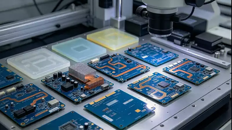
PCB insert molding places a prefabricated circuit board into a mold before molten plastic is injected around selected areas. After cooling, the molded plastic mechanically integrates the board into a larger component or product structure.
This injection molding circuit board method is appropriate when a conventional PCB needs to be held securely within a custom-shaped plastic part. It can reduce the need for separate brackets or fastening features, depending on the design. The mold must position the board accurately and prevent movement during injection.
Engineers should evaluate the PCB substrate, component packages, solder joints, and exposed contacts before choosing insert molding. Temperature, injection pressure, and polymer flow may damage sensitive components or place stress on soldered connections. Mold geometry and gate placement should be designed to control these risks.
Connectors, test points, antennas, and other functional interfaces may need to remain exposed. Their locations should be specified before tooling begins so that the molded structure does not block electrical connections or prevent inspection.
Circuit board overmolding
Circuit board overmolding involves applying plastic around an existing PCB or electronic assembly. Depending on the product requirements, the polymer may cover only selected regions or enclose most of the board.
An overmolded circuit board can benefit from improved mechanical support, strain relief, and integration with the product housing. However, the process must account for the temperature limits of electronic components, the strength of solder joints, and the compatibility of the molding material with the existing assembly.
When designing an injection molding circuit board for overmolding, engineers should identify areas that must remain accessible for connectors, sensors, heat transfer, and testing. They should also consider whether the finished assembly needs repair or component replacement. Permanent encapsulation can make later repairs difficult or uneconomical.
Molded interconnect devices and in-mold electronics
Molded interconnect devices (MIDs) and in-mold electronics (IME) take a different approach. Rather than simply enclosing a conventional PCB, these technologies integrate conductive features or electronic functions into shaped plastic structures.
A MID can use specialized processes to create conductive paths on a three-dimensional molded surface. IME commonly combines printed conductive patterns and electronic components on a formable film with forming and molding operations. Both approaches require the electrical layout and mechanical geometry to be considered together.
These technologies may be suitable for curved control panels, integrated lighting, touch interfaces, and compact electronic surfaces. They are not interchangeable with conventional PCB insert molding, so the choice should reflect circuit complexity, product shape, production volume, and performance requirements.
Material Selection and Design Requirements
Material selection is a critical part of injection molding circuit board development. The polymer must meet the mechanical and environmental requirements of the product without compromising the PCB or its components.
Thermoplastics used in injection molding differ in processing temperature, shrinkage, stiffness, chemical resistance, and dimensional stability. The chosen material must be compatible with the board substrate, component packages, solder joints, and any surface treatments. Where adhesion or sealing is required, the interface between the plastic and the electronic assembly also needs evaluation.
The molding process can expose the circuit board to heat, pressure, and mechanical loading. Engineers should review component placement, board support, mold flow, and gate location to reduce the risk of deformation or damage. Prototype trials can help identify problems before production tooling is finalized.
Electrical design remains equally important. An injection molding circuit board may include high-speed signals, RF circuits, sensors, or power components that require specific clearances and grounding arrangements. Plastic geometry can change the surrounding electromagnetic environment, particularly for antennas and RF structures. Designs with critical signal integrity or wireless performance should be validated in the final molded configuration rather than assessed only as a bare PCB.
Thermal management also requires attention. Plastic may restrict airflow or change the path through which heat leaves the board. Components with significant power dissipation may need exposed thermal surfaces, heat spreaders, or other dedicated cooling provisions. Encapsulation should not be assumed to improve thermal performance simply because it protects the electronics.
Manufacturing and Quality Testing
Reliable injection molding circuit board production requires coordinated control of PCB fabrication, electronic assembly, mold preparation, injection conditions, and final inspection. Problems introduced during any stage can affect both electrical performance and mechanical integrity.
Before molding, the PCB and assembled components should be inspected for placement accuracy, soldering defects, and damage. The mold must hold the insert in the correct position, while the selected injection conditions must be suitable for the materials and components. After molding, the assembly should be checked for deformation, incomplete filling, surface defects, exposed-interface accuracy, and dimensional consistency.
Electrical testing is necessary to confirm that the injection molding circuit board still performs as intended. Continuity and isolation tests can identify open connections or unintended shorts, while functional testing verifies the behavior of the complete electronic assembly. Depending on the application, additional checks may cover connector integrity, sensor operation, RF performance, sealing, or resistance to vibration and temperature changes.
Testing access should be considered before the board is encapsulated. If test points and critical connections become inaccessible after molding, manufacturers may need to perform more verification before the molding stage or design dedicated test interfaces into the assembly.
For production programs, process validation and repeatability are important. Material batches, molding parameters, insert positioning, and inspection criteria should be controlled to reduce variation between units. The appropriate qualification plan depends on the product’s operating environment and reliability requirements.
Applications and Selection Considerations
An injection molding circuit board can support products that need electronics integrated into a compact or nontraditional mechanical form. Potential applications include automotive interior controls, molded sensor housings, consumer electronics, smart interfaces, and electronic components that require additional mechanical protection.
The best integration method depends on the purpose of the molded structure. PCB insert molding may be suitable when a conventional board must become part of a larger plastic component. PCB overmolding may be considered when selected areas of an electronic assembly need protection or strain relief. MID and IME technologies may be more appropriate when electrical functions must follow a three-dimensional surface.
Manufacturing volume is another consideration. Custom molds and specialized processes can require significant upfront investment, so the economics differ between prototypes and high-volume production. Designers should also consider repairability, inspection access, material availability, and the cost of validating the final assembly.
A successful injection molding circuit board project balances electrical function, material compatibility, mechanical design, and manufacturing repeatability. Defining the required interfaces early, choosing the appropriate integration process, and validating the complete molded assembly help ensure that the final product meets its functional and reliability requirements.