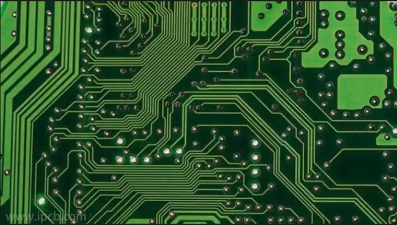
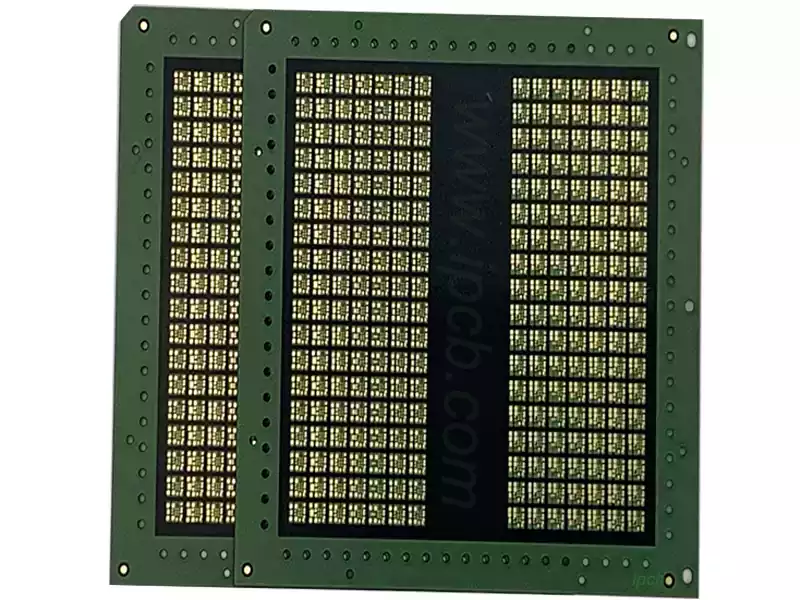
A multilayer metal core PCB combines the routing capacity of a multilayer circuit board with the thermal spreading capability of a metal substrate. Instead of relying entirely on conventional organic laminate materials, the board incorporates a conductive metal core, typically aluminum or copper, together with electrically insulating dielectric layers and multiple copper circuit layers. This construction is useful when a circuit requires more routing space while also dealing with significant heat generation. The metal core can provide a direct thermal spreading path and additional mechanical support, while the multilayer circuit structure allows power, ground, and signal networks to be distributed across different layers.
How a Multilayer Metal Core PCB Is Structured
The structure of a multilayer metal core PCB depends on the electrical and thermal requirements of the design. A typical construction includes several copper circuit layers separated by dielectric materials, with an aluminum or copper core positioned within or beneath the circuit stack. The dielectric layer has an important dual role: it electrically isolates the copper circuitry from the conductive metal core while providing a thermal path between the circuit and the metal substrate. This means its thermal conductivity and thickness can directly affect the overall thermal performance of the board.
The metal core itself is not simply another conductive layer in the circuit. Its main function is generally to spread heat away from high-power components and distribute that heat toward a larger thermal area or an external heatsink. Aluminum is widely considered when lower weight and practical thermal performance are important, while copper can be selected when higher thermal conductivity and current-carrying or mechanical requirements justify its greater density and material cost. The appropriate choice depends on the complete thermal and electrical design rather than on the metal alone.
Multilayer construction becomes useful when a single or double copper layer cannot provide enough routing space for the circuit. Additional layers can separate power and signal networks, provide dedicated reference or ground planes, and reduce routing congestion. At the same time, however, every additional dielectric interface between a heat-generating component and the metal core can influence the thermal path. A multilayer metal core PCB therefore cannot be designed by treating the electrical stack-up and thermal structure as two independent problems.
Thermal Management in Multilayer Metal Core PCB Design
Thermal management is one of the main reasons to consider a metal core PCB, but the presence of a metal core does not automatically guarantee effective heat dissipation. The complete heat path must be considered from the component junction through the component package, solder interface, copper land, dielectric material, metal core, and finally to the heatsink or surrounding environment. If one section of this path introduces excessive thermal resistance, the benefit of the metal substrate can be reduced.
This becomes particularly important in multilayer designs. A component mounted on an outer copper layer may be separated from the metal core by one or more dielectric layers and internal copper structures. The designer therefore needs to determine where the highest heat loads occur and how efficiently those regions can transfer heat toward the metal core. A thermally conductive dielectric can improve this path, but its thickness, dielectric strength, mechanical properties, and compatibility with the manufacturing process also need to be considered.
The relationship between copper routing and thermal management is equally important. Wider copper areas can help spread heat and reduce electrical resistance, while thermal vias or other engineered heat-transfer structures may be used where the manufacturing stack-up allows them. When a conductive metal core is present, however, vias cannot simply be connected to the core without considering electrical isolation. Depending on the construction, the metal core may need clearance around drilled holes or specially designed insulated transitions so that interlayer connections do not create unintended electrical shorts. Metal-core PCB manufacturing therefore requires closer coordination between the PCB layout and fabrication process than a conventional multilayer FR-4 board.
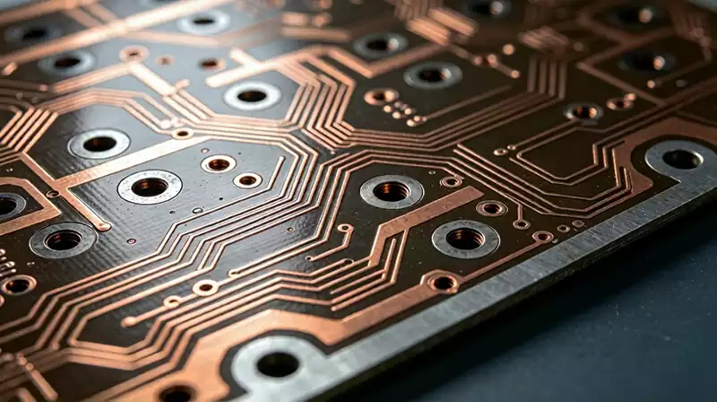
Manufacturing Considerations for Multilayer Metal Core PCBs
Manufacturing a multilayer metal core PCB begins with preparing the metal substrate and the dielectric bonding system. The metal surface needs to be suitable for reliable bonding, after which the dielectric and copper layers are assembled according to the specified stack-up. Precise alignment becomes important because the metal core occupies a conductive region of the structure and cannot be treated exactly like a conventional insulating FR-4 core.
The drilling and interconnection stages can also require special treatment. In a conventional multilayer PCB, plated through-holes can pass through insulating laminate relatively directly. In a metal-core construction, a drilled hole that reaches the conductive core could create an electrical connection that the circuit does not intend. One manufacturing approach is therefore to create an isolated region around the hole in the metal layer and use an insulating material or other isolation structure before completing the plated interconnection. The exact method depends on the stack-up and manufacturing technology.
After the multilayer structure has been laminated and the required interconnections have been formed, the remaining PCB fabrication stages can include circuit imaging and etching, copper plating, solder mask application, surface finishing, electrical testing, and dimensional inspection. Lamination itself deserves particular attention because the board combines materials with different thermal and mechanical properties. Differences in expansion behavior, bonding conditions, layer alignment, and metal thickness can affect warpage, registration, and long-term reliability.
For this reason, manufacturability should be considered before the final PCB layout is completed. The designer needs to establish the metal core position, dielectric thickness, copper weights, via structures, clearances, board thickness, and thermal requirements as part of one stack-up rather than specifying them independently. A design that works electrically but creates an impractical thermal path or difficult isolation structure may require substantial changes before production.
Where Multilayer Metal Core PCBs Are Used
Multilayer metal core PCBs are particularly relevant to electronic assemblies where circuit density and heat generation occur at the same time. Power electronics, LED systems, automotive electronics, motor control, industrial equipment, and other high-power applications are common examples discussed in current technical references. In these applications, the multilayer structure provides additional space for power and signal routing, while the metal core provides a thermal spreading path.
The technology is not intended to replace conventional multilayer PCBs in every design. When heat generation is modest, a conventional laminate may provide a simpler manufacturing solution. A multilayer metal core PCB becomes more relevant when the electrical complexity of the circuit requires multiple copper layers and the thermal load makes a conventional organic substrate less suitable.
The most important design principle is to treat the board as a complete electrical, thermal, and mechanical system. Metal selection, dielectric properties, layer count, component placement, copper distribution, via structures, and the final thermal interface all influence performance. By defining these factors together during stack-up and layout development, a multilayer metal core PCB can provide additional routing capability without losing sight of the thermal requirements that led to the metal-core construction in the first place.