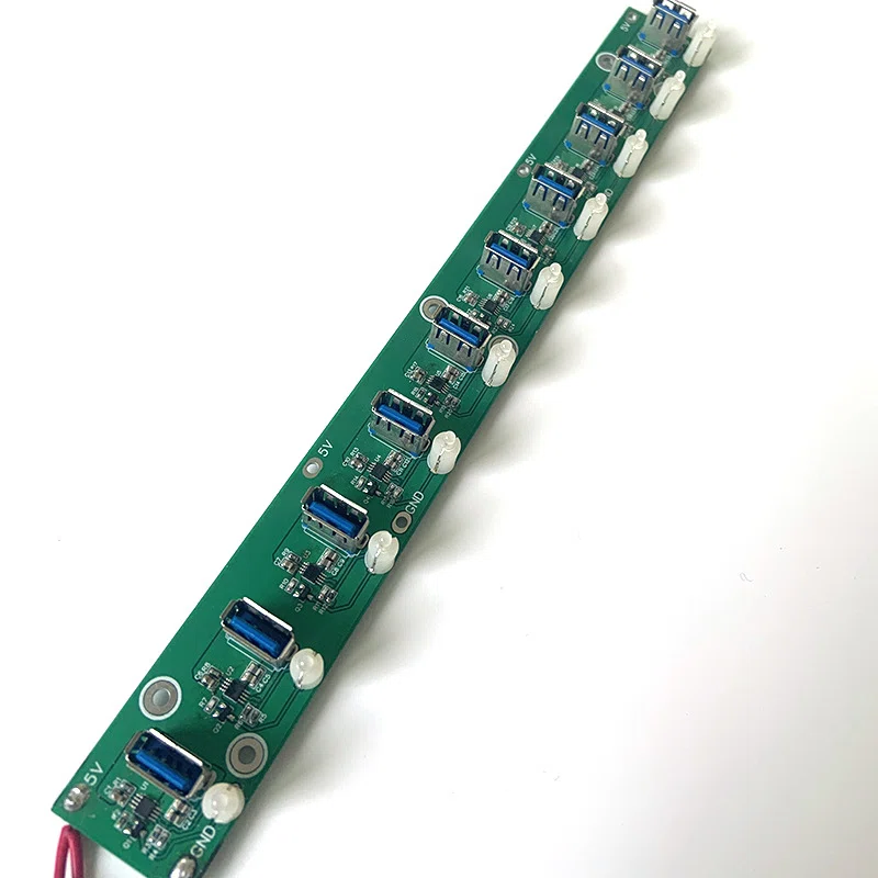
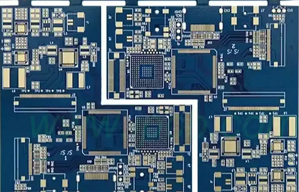
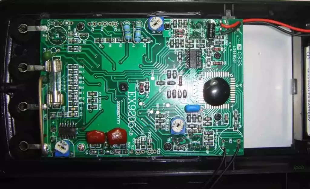
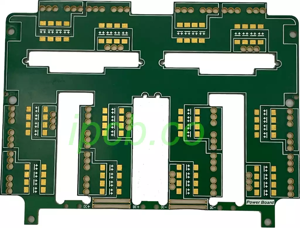
Designing circuit boards involves converting an electronic design concept into a physical structure that connects components and allows the system to operate as intended. A PCB is more than a carrier for electronic components. The arrangement of copper traces, power networks, signal paths, layer structures, and component locations directly affects electrical performance, reliability, and production feasibility.
A PCB design must satisfy both circuit requirements and manufacturing conditions. Engineers need to consider signal transmission, power distribution, thermal behavior, mechanical limitations, and production processes during development. The final board is the result of decisions made throughout the design process, from the initial schematic to the finished layout.
The Basic Process of Designing Circuit Boards
The design process usually starts with defining the requirements of the electronic product. Engineers first determine the circuit functions, required components, operating conditions, power requirements, signal characteristics, and available installation space.
After the requirements are confirmed, the schematic is created. The schematic describes the electrical relationship between components such as integrated circuits, resistors, capacitors, connectors, and power devices. It defines how the circuit works, while the PCB layout determines how those connections are physically implemented on the board.
Once the schematic has been verified, the design moves into PCB layout. Engineers assign component footprints, arrange components on the board, and create copper routing between connections. At this stage, placement decisions influence many later factors, including signal quality, heat distribution, routing difficulty, assembly efficiency, and testing accessibility.
Different circuit sections usually require different layout considerations. High-speed devices may need shorter connections to reduce signal distortion, while power components may require additional copper areas or thermal structures. Sensitive analog or RF circuits often need separation from switching circuits and other potential noise sources.
Component Placement and PCB Layout Design
Component placement creates the foundation for the entire PCB layout. A poorly planned arrangement can increase routing complexity, extend signal paths, and create additional electromagnetic interference concerns.
Engineers normally organize components according to their electrical functions. Power circuits, processing units, communication interfaces, and control sections are often arranged in related areas to simplify routing and improve current flow. This approach also makes later debugging and testing easier.
Thermal conditions are another factor that affects placement. Components with higher power consumption generate more heat and may require larger copper areas, thermal vias, or additional cooling structures. Placing heat-generating components too close to temperature-sensitive devices can affect long-term reliability.
After placement is completed, traces are routed between components. The routing strategy depends on factors such as circuit complexity, layer count, operating frequency, and electrical requirements.
Simple designs may use single-layer or double-layer boards, while more complex electronic systems often require multilayer PCBs. Additional layers provide more routing space and allow designers to separate signal, power, and ground structures. This is especially useful for high-density circuits and high-speed electronic products.
Signal Integrity and Manufacturing Considerations
As electronic systems operate at higher speeds, PCB design requires more attention to signal integrity. A copper trace carrying a high-speed signal is not simply a physical connection between two components. Its electrical behavior is influenced by trace geometry, dielectric materials, layer arrangement, and the surrounding reference structures.
Controlled impedance is an important factor in many high-speed PCB designs. Parameters such as trace width, copper thickness, dielectric thickness, and material properties affect the impedance of a transmission line. If the manufactured board differs significantly from the intended design structure, issues such as signal reflection, transmission loss, or timing errors may occur.
The PCB stack-up plays an important role in maintaining signal performance. A properly designed multilayer structure can provide dedicated signal layers, stable reference planes, and improved power distribution. This approach is commonly used in applications involving processors, memory interfaces, communication circuits, and other high-speed electronic systems.
However, electrical performance is only one part of the design process. A PCB layout also needs to meet manufacturing requirements. A design may function correctly in theory but still create production difficulties if it contains extremely narrow traces, insufficient spacing, complex via structures, or an unsuitable layer arrangement.
Design for manufacturability (DFM) helps identify these issues before production begins. During a DFM review, engineers typically evaluate factors such as minimum trace width, spacing requirements, hole sizes, solder mask openings, surface finishes, layer registration, and assembly conditions.
Considering manufacturing limitations during the design stage can reduce unnecessary redesign work and improve production consistency. The connection between PCB design and manufacturing is especially important for complex boards with high layer counts, dense components, or strict electrical requirements.
Common Challenges When Designing Circuit Boards
One of the main challenges in designing circuit boards is balancing electrical requirements with physical limitations. Modern electronic products often require more functions within smaller spaces, which creates pressure on routing density, thermal management, and component arrangement.
Power distribution is an important consideration in many PCB designs. Circuits may contain multiple voltage levels and sections that handle significant current. Poor power routing can increase voltage drop, introduce unwanted noise, or affect system stability. Proper power planes, grounding methods, and decoupling capacitor placement help maintain a stable power supply.
Electromagnetic interference is another issue that needs to be addressed during PCB layout. Electronic circuits naturally generate electromagnetic energy, and improper routing or grounding can allow unwanted coupling between different sections of the circuit.
Designers may use methods such as appropriate layer planning, controlled return paths, shielding structures, and component separation to reduce interference. These methods are most effective when considered early in the design process rather than added after layout completion.
Testing and maintenance requirements should also influence PCB design decisions. Adding suitable test points, organizing functional areas clearly, and considering assembly requirements can improve production testing efficiency and make future troubleshooting easier.
Before a PCB enters manufacturing, engineers often perform design verification through methods such as design rule checking, electrical analysis, signal evaluation, and manufacturability reviews. These checks help identify potential problems before they become production issues.
From PCB Design to Reliable Manufacturing
Designing circuit boards is a process that connects electrical concepts with physical manufacturing. The purpose is not simply to create connections between components but to develop a board structure that can operate reliably in real applications.
A complete PCB design considers the entire product development process, including circuit requirements, component selection, layout planning, manufacturing conditions, assembly processes, and testing requirements.
Factors such as signal performance, thermal behavior, mechanical restrictions, and production capability all influence the final result. A design that performs well electrically but cannot be manufactured efficiently may require further optimization before production.
As electronic products become more compact and functionally complex, designing circuit boards play a greater role in determining product reliability and performance. A carefully developed circuit board provides stable electrical connections, supports efficient manufacturing, and helps ensure consistent operation throughout the product lifecycle.