PCB copper thickness refers to the thickness of the copper foil in the printed circuit board (PCB), is an important parameter of the circuit board. It is used for PCB conductive, is precipitated in the circuit board substrate layer of a thin, continuous layer of metal foil. PCB copper thickness is divided into the inner layer of copper thickness and outer layer of copper thickness, generally expressed in OZ (ounces). 1oz means that the weight of 1oz of copper uniformly spread in an area of 1 square feet (FT2) to achieve the thickness. It is the weight per unit area to indicate the average thickness of copper foil, expressed in the formula that is, 1oz = 28.35g / FT2. (FT2 and SQFT for square feet, 1 square foot = 0.09290304 square meters).
1oz represents the PCB copper foil thickness of about 35um.
International PCB copper skin thickness commonly used are: 35um,50um,70um.
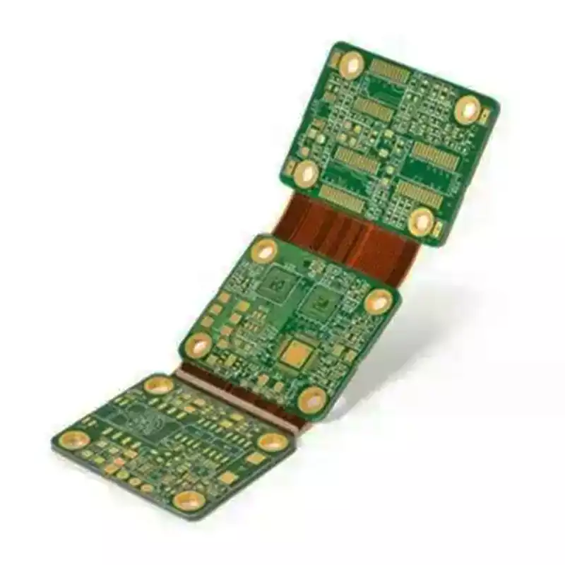
PCB circuit board inner and outer layer copper thickness
Outer copper thickness: usually refers to the thickness of the conductive layer visible on the surface of the PCB.This part of the copper foil is mainly used to carry external components of the pad, alignment, etc., direct contact with the components and realize the electrical connection.The outer layer of copper thickness is generally set according to the actual application requirements, common specifications are 0.5 ounces (about 17.5 microns),1 ounce (about 35 microns) to 2 ounces (about 70 microns) ranging.
Inner Copper Thickness: Inner copper thickness refers to the thickness of the copper foil on the non-exposed level inside the PCB substrate. These copper layers, which are hidden in the dielectric layer, are responsible for building complex circuit networks that electrically interconnect the different layers. The options for inner layer copper thickness are equally varied, but tend to be on the thinner side compared to the outer layer, with common specifications of 0.5 ounces or thinner.
General single and double-sided PCB board copper foil (copper cladding) thickness of about 35um (1.4mil), another specification for the 50um and 70um. multilayer board surface layer thickness is generally 35um = 1oz (1.4mil), the inner layer of 17.5um (0.7mil). 70% of the circuit boards used to complete the thickness of the 35um copper foil, which depends mainly on the PCB’s purpose and signal Voltage, current size; In addition, for the PCB to be over the high current, part of the copper thickness will be used to 70um, 105um copper thickness, and rarely 140um and so on. Higher copper thickness can provide better current carrying capacity and thermal conductivity, but will also increase the cost and weight of the board. Choosing the right copper thickness should be based on the circuit’s power requirements, line width and spacing requirements.
Usage is different, the thickness of the copper skin is also different, ordinary 0.5oz, 1oz , 2oz, mostly used in consumer and communications products. 3oz or more is a thick copper products, mostly used for high current, such as high-voltage products, power supply boards!
PCB copper thickness of the factors affecting in-depth analysis
Electrical Characteristics: The copper thickness of PCB is a key factor affecting its current carrying capacity and impedance regulation. A thicker copper layer means a larger conductive area, so it can withstand higher currents and reduce resistance and voltage losses, thus ensuring the stability and efficient operation of the circuit. Especially in high-frequency circuits or high-current applications, such as power supply and RF circuits, a moderate increase in copper thickness can effectively reduce energy loss and improve signal integrity.
Thermal performance: Copper’s excellent thermal conductivity makes copper thickness an important factor in PCB thermal performance. Increasing the copper thickness means expanding the heat dissipation area, thus more effectively dispersing the heat generated by the components to the heat sink or housing, lowering the operating temperature and improving the reliability of the product. Choosing the right copper thickness is critical for high power devices or electronic products that require efficient thermal management.
Mechanical strength: The copper layer plays a role in enhancing the structural stability of the PCB board. For large component-free areas or large PCBs, sufficient copper thickness prevents board deformation or fracture during processing, assembly and use. In addition, a thicker copper layer improves the connection strength of solder joints and reduces the risk of poor soldering.
Cost and Processing Challenges: However, thicker copper is not always better. Excessively thick copper layers can increase material costs, manufacturing difficulties and scrap rates. For example, the etching process takes longer and requires higher energy, which can lead to over- or under-etching; and lamination requires more pressure to ensure a tight bond between layers, which can place an additional burden on equipment. At the same time, thick copper plates are also prone to burrs and delamination during drilling and cutting processes. Therefore, under the premise of meeting the performance requirements, the copper thickness should be reasonably selected to balance the cost-effectiveness.
Design Limitations: Different PCB design software and manufacturers have certain copper thickness requirements. A copper layer that is too thick or too thin may exceed its handling capacity, making the design unachievable or difficult to produce. In addition, too thick a copper layer may also cause electromagnetic compatibility problems, which need to be solved by reasonable grounding design and shielding measures.
Copper Foil Properties
Copper foils have low surface oxygen characteristics and can be attached to a variety of substrates, such as metals, insulating materials, etc., and have a wide temperature range. Mainly used in electromagnetic shielding and anti-static, the conductive copper foil is placed on the backing surface, combined with the metal substrate, has excellent conductivity and provides electromagnetic shielding effect. It can be categorized into: self-adhesive copper foil, double-conducting copper foil, single-conducting copper foil and so on.
Electronic grade copper foil (purity 99.7% or more, thickness 5um-105um) is one of the basic materials of the electronic industry electronic information industry is developing rapidly, the use of electronic grade copper foil is increasing, the products are widely used in industrial calculators, communication equipment, QA equipment, lithium-ion batteries, civilian TV sets, VCRs, CD players, photocopiers, telephones, heating and air conditioning, automotive electronic components, game consoles and so on. components, game consoles, etc.
There is an increasing demand for electronic grade copper foil,especially high-performance electronic grade copper foil,in both domestic and overseas markets. Relevant organizations predict that by 2015,China’s domestic demand for electronic-grade copper foil will reach 300,000 tons,and China will become the world’s production base for printed wiring boards and copper foil, so the market for electronic-grade copper foil, especially high-performance foil, is promising.
PCB copper thickness as an important parameter of the printed circuit board,the choice of not only the electrical performance,heat dissipation ability,but also affect the mechanical strength, cost and processing difficulty and other aspects.In high-frequency circuits, high-current applications or high-power devices, an appropriate increase in copper thickness can effectively improve circuit stability and thermal efficiency.However,too thick a copper layer may also lead to increased costs and processing difficulties. Therefore, in PCB design, the rational choice of copper thickness is particularly important.In the pursuit of performance, but also need to consider the cost-effectiveness and production feasibility, in order to achieve the best performance and economic benefits of the circuit board.