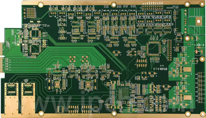
In the PCB manufacturing industry, broken circuit board traces are a recurring challenge at every stage, from production and testing through to transport and subsequent use. The causes are varied—they may include localised breaks resulting from improper soldering, traces coming loose due to external impact, disconnections caused by ageing or corrosion following prolonged use, or stress concentrations arising from design flaws.
Repairing circuit board traces is by no means simply a matter of ‘reconnecting’ them; rather, it requires ensuring electrical continuity whilst simultaneously maintaining signal integrity, thermal dissipation performance and mechanical strength, thereby preventing issues such as secondary breaks or signal interference following repair.
Repair strategies vary depending on the type of circuit board and the location of the break: fine traces on high frequency circuit boards require attention to impedance matching; thick traces on high-power circuit boards demand enhanced heat dissipation and current-carrying capacity; whilst dense traces on precision circuit boards necessitate strict control over operational precision to avoid damaging adjacent components.
Accurate diagnosis is the prerequisite for repair. Blind operation not only fails to repair the break but may also cause further damage to pads and components, or even trigger short circuits. In circuit board repair practice, we consistently adhere to the principle of ‘diagnose first, classify next, then repair’, ensuring that every step is targeted and precise, thereby enhancing repair efficiency and success rates.
Methods for Troubleshooting Broken Circuit Board Traces
Initial Inspection: Begin by visually inspecting the surface of the circuit board, paying particular attention to areas prone to breakage such as around pads, trace bends, and component lead connections, to make an initial assessment of the location and length of the break.
Precise Localisation: For minute breaks that are difficult to detect with the naked eye (such as breaks in inner layer traces or hidden breaks caused by surface oxidation), tools such as a multimeter or oscilloscope must be used to measure continuity and signal transmission, thereby pinpointing the exact location of the break.
Comprehensive Assessment: At the same time, it is necessary to check whether there are any issues in the vicinity of the break, such as damaged components, detached pads or oxidised traces. If these issues are not addressed simultaneously, the fault is highly likely to recur after repair.
Based on the location, length, trace specifications and pcb board type, trace breaks can be categorised into three types, each with distinct repair priorities:
Surface trace breaks: Breaks in the top layer of the pcb circuit board, typically less than 5 mm in length, with no components obstructing the surrounding area. This is the most common type and presents the lowest repair difficulty.
Trace breaks in dense areas: These are frequently found on precision circuit boards (such as those in mobile phones and medical devices), where traces are fine, spacing is tight, and the surrounding area is densely populated with components. Repair requires extremely high precision, and great care must be taken to avoid damaging adjacent components.
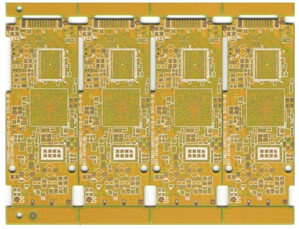
Inner-layer trace breaks: These occur within the inner layers of the circuit board, are invisible to the naked eye, and are difficult to locate. Repair requires specialised equipment and a high level of technical skill, and is most commonly found on multi-layer circuit boards.
Furthermore, repair standards must be determined based on the PCB’s application: in high-reliability sectors such as industrial control and automotive electronics, repairs must meet the original manufacturer’s standards and may even require ageing tests; whereas for standard consumer electronics, restoring normal functionality is sufficient. Clarifying the diagnosis results and repair standards forms the basis for selecting the appropriate method.
Repair Methods:
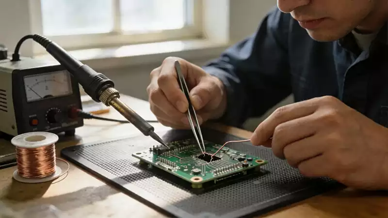
1.Wire Soldering Repair Method: A basic, general-purpose method suitable for superficial short breaks
This is the most basic and commonly used method, suitable for scenarios where surface traces are broken, the length of the break is between 1 and 5 mm, and there are no obstructions in the surrounding area, such as surface traces on standard consumer electronics or industrial control boards.
Procedure:
Cleaning: Wipe both ends of the break with sandpaper or alcohol to remove the oxide layer and ensure the metal surface is clean.
Prepare the wire: Cut a length of fine copper wire with the same gauge as the original trace, slightly longer than the gap between the breaks.
Soldering: Align both ends of the copper wire with the ends of the trace. Use a soldering iron (set to 260–300°C) with flux to solder the connection, ensuring the joint is secure and free from cold solder joints.
Cleaning and Testing: Remove any residual flux with alcohol and use a multimeter to verify electrical continuity.
Precautions: Do not heat for more than 3 seconds at a time to avoid damaging the substrate with excessive heat; the gauge of the copper wire must match that of the original trace, as a wire that is too thick will result in current-carrying capacity mismatch, whilst one that is too thin is prone to breaking again.
2.Jumper Wire Repair Method: A flexible alternative, suitable for long cracks or densely populated areas
This method is suitable for broken traces in densely populated areas, surface breaks longer than 5 mm, or situations where the original trace cannot be soldered directly, such as repairs to precision circuit boards or mobile phone boards. The core principle involves using fine enamelled wire to replace the original trace for the transmission of signals and current.
Procedure:
Preparation: Clean the pads at both ends of the break. Select fine enamelled wire with a matching gauge and carefully strip the insulation from both ends using wire strippers.
Soldering: Solder the two ends of the enamelled wire to the pads at either end of the broken trace. If components are densely packed in the surrounding area, use high-temperature tape to lift and secure the enamelled wire off the surface to prevent contact and short circuits.
Insulation: Apply insulating compound to the solder joints to prevent short circuits during subsequent use.
Key Points: The jumper route should follow the original trace as closely as possible to minimise signal loss. Particularly in high-frequency circuits, the length of the jumper must be strictly controlled to avoid impedance mismatch and signal interference.
3.Wire Replacement Repair Method: A professional technique specifically for repairing internal layers or large-area breaks
Suitable for scenarios involving broken internal traces, damage to multilayer pcb boards, or extensive damage to surface traces. This repair method is highly complex and requires specialised equipment; it is primarily used for high-end PCB boards in industrial control and medical devices.
Procedure:
Precise Localisation: Use X-ray inspection equipment to determine the exact location and length of the internal layer break.
Window Creation: Use a laser patching machine to create micro-channels on the PCB surface, reaching both ends of the internal layer break.
Filling and Conductivity: Inject conductive silver paste into the channels to cover the break. Once the silver paste has cured, electrical connectivity is restored.
Insulation and Testing: An insulating coating is applied for protection, and finally, a multimeter and oscilloscope are used to verify continuity and signal quality.
Note: This method demands extremely high standards of equipment and operational skill, and the repair costs are also high; therefore, it is only suitable for circuit boards of high value and with high reliability requirements.
4.Integrated Pad and Trace Repair Method: Combined Repair for Composite Damage
Suitable for scenarios where a broken trace is accompanied by a detached pad, commonly caused by soldering errors or physical impact. If only the trace is repaired whilst the pad is neglected, components cannot be soldered and the circuit board will remain inoperable.
Procedure:
Repairing the pad: Clean the substrate at the detached area, cut a piece of copper foil matching the size of the original pad, secure it with conductive adhesive, and then reinforce it with solder.
Repairing the trace: Following the wire soldering method or jumper wire repair method, reliably connect the broken trace to the new pad.
Inspection: Confirm that the pad is level and the trace is conductive, ensuring that subsequent components can be soldered correctly.
Detailed Control of the Repair Process
Selection of Tools and Materials:
Soldering iron: A constant-temperature model must be used to prevent temperature fluctuations.
Solder wire: Give preference to lead-free, environmentally friendly types; the melting point must be compatible with the substrate.
Wires: The gauge and material (oxygen-free copper recommended) of fine copper wire or enamelled wire should match the original traces to ensure current-carrying and signal performance.
Flux/silver paste: Select a non-corrosive, no-clean flux; conductive silver paste must possess good conductivity and curing strength.
Operational Standards:
Thoroughly clean the circuit board before repair to remove oxidation and contaminants.
Strictly control temperature and time during soldering to prevent damage from excessive heat.
Remove all residues after repair to avoid the risk of short circuits.
Post-Repair Protection:
Reinforcement: Apply insulating adhesive to the repaired area; once cured, this forms a protective layer and enhances mechanical strength. For areas subject to stress, reinforce with high-temperature tape.
Environmental Protection: For circuit boards used outdoors or in harsh environments, moisture-proof and anti-corrosion treatments must be applied to extend their service life.
Comprehensive Testing:
Continuity Testing: Use a multimeter to confirm there are no cold solder joints or false solder joints.
Signal Testing: For high-frequency boards, use an oscilloscope to check signal integrity, ensuring there is no attenuation or interference.
Current-Carrying Capacity Testing: For high-power boards, verify that the repaired area can withstand the rated current without abnormal heating.
Ageing Test: Simulate actual operating conditions to ensure the repaired circuit board can operate stably over the long term.
The essence of circuit board repair lies not only in restoring functionality but also in rebuilding trust. From precise troubleshooting to meticulous protection, every step of rigorous operation represents a commitment to the long-term, stable operation of the circuit board. True professionalism lies not merely in knowing how to repair, but in ensuring that the repair stands the test of time.