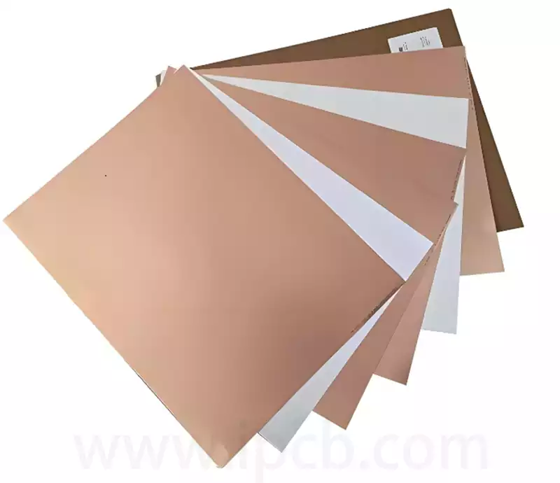
When designing and manufacturing PTFE high-frequency PCBs, engineers typically focus on dielectric constant, dissipation factor, substrate thickness, and impedance control. Copper foil selection, however, also plays an important role in the electrical performance of the finished board. At microwave and millimeter-wave frequencies, current flows primarily near the conductor surface. As a result, the microscopic surface profile of the copper foil can affect conductor loss. Even when two PCBs use the same PTFE substrate and copper thickness, different copper foil types or surface finishes may produce different insertion loss results.
Two commonly used copper foil types in PTFE copper-clad laminates are rolled annealed copper (RA copper) and electrodeposited copper (ED copper). Because they are manufactured using different processes, they have different grain structures, surface profiles, and mechanical properties. RA copper generally offers good ductility and can be manufactured with a relatively smooth surface. ED copper is produced through an electrochemical deposition process, with its surface characteristics adjusted through subsequent treatments.
Choosing between RA and ED copper requires more than looking at the foil designation. For PTFE high-frequency PCBs, engineers should also consider the roughness of the copper surface that contacts the dielectric, the surface treatment, the bonding strength after lamination, and the requirements of the finished application.
How Are RA Copper and ED Copper Manufactured?
RA copper is produced through mechanical rolling followed by annealing. During manufacturing, copper is passed through a series of rolling stages to reduce its thickness. Annealing then helps adjust its internal structure and mechanical properties. The rolling process elongates the copper grains along the working direction, which generally gives RA copper good elongation and flexibility. These properties make it a useful option for circuits that must withstand mechanical deformation or repeated bending.
The surface of RA copper is generally smooth, although its actual roughness depends on the rolling process, foil thickness, and subsequent surface treatment. Some RA products are specifically manufactured with a low-profile surface for high-frequency applications. However, a smoother surface does not automatically guarantee sufficient adhesion to PTFE. The final bonding performance also depends on the copper treatment and lamination conditions.
ED copper is manufactured through an electrochemical deposition process. Copper ions are reduced and deposited onto a rotating cathode drum, gradually forming a copper foil of the required thickness. The two sides of the foil may have different surface characteristics. The side in contact with the drum is generally smoother, while the opposite side can be further treated to achieve the surface properties required for a particular application.
Conventional ED copper foil may undergo roughening treatment to improve bonding with the substrate. However, excessive surface roughness can increase conductor loss at high frequencies. To address this issue, copper foil manufacturers have developed low-profile products such as VLP (Very Low Profile) and HVLP (Hyper Very Low Profile) copper foil. These products are designed to control surface roughness while maintaining suitable bonding performance.
For this reason, it would be inaccurate to assume that all ED copper foils have rough surfaces or that RA copper is always the better choice for high-frequency applications. The performance of a specific foil grade must be evaluated using its actual surface characteristics and electrical data.
Key Performance Differences Between RA and ED Copper on PTFE Boards
The main differences between RA and ED copper involve their manufacturing processes, surface profiles, mechanical properties, and suitability for different PCB structures. For PTFE high-frequency applications, engineers must also consider how the copper foil bonds to the dielectric material.
| Parameter | RA Copper | ED Copper |
|---|---|---|
| Manufacturing process | Mechanical rolling followed by annealing | Electrochemical deposition |
| Grain structure | Grains are generally elongated along the rolling direction | Grain structure depends on deposition conditions |
| Surface profile | Generally smooth, depending on foil grade and treatment | Can be adjusted through deposition and surface treatment |
| High-frequency performance | Low-profile surfaces can help reduce conductor loss | Performance varies between standard ED, VLP, and HVLP grades |
| Ductility | Generally offers good elongation | Depends on foil grade and manufacturing process |
| Flexibility | Often suitable for applications involving repeated bending | Must be evaluated based on elongation and bending requirements |
| Substrate adhesion | Requires appropriate surface treatment and lamination conditions | Roughening and other treatments can improve bonding |
| Cost and availability | Depends on thickness, grade, and supplier | Available in a wide range of specifications, with established volume supply options |
Surface roughness deserves particular attention when evaluating high-frequency performance. RA copper generally offers a smoother surface, while conventional ED copper may have a more pronounced surface profile. However, the difference is not necessarily significant when RA copper is compared with VLP or HVLP ED copper. Engineers should review the roughness specifications of the actual products rather than relying solely on their copper foil classifications.
How Copper Foil Roughness Affects Signal Loss in PTFE High-Frequency PCBs
At high frequencies, current distribution in a conductor is affected by the skin effect. As frequency increases, current becomes increasingly concentrated near the conductor surface. The depth over which most of the current flows is known as the skin depth, which generally decreases as frequency rises. Under these conditions, microscopic variations in the copper surface can have a greater influence on the current path.
If the copper surface contains pronounced peaks, valleys, or irregularities, the actual current path may become more complex than it would be on an ideal smooth surface. This can increase conductor loss. The effect is particularly relevant in PTFE PCBs operating in the millimeter-wave range. It deserves close attention in designs with long transmission lines, tight insertion loss budgets, or demanding phase and amplitude requirements.
RA copper generally offers a relatively low surface roughness, which can help reduce the influence of surface irregularities on high-frequency signal transmission. However, this does not mean that RA copper will always outperform ED copper at every frequency or in every PCB structure. Low-profile ED copper, particularly VLP and HVLP grades, can also meet the requirements of many high-frequency applications. Actual performance depends on several factors, including copper thickness, trace geometry, surface treatment, dielectric thickness, and operating frequency.
It is also important to identify which side of the copper foil is being measured. In a PTFE copper-clad laminate, the copper surface in contact with the dielectric is often more relevant to both signal transmission and interfacial bonding than the exposed surface. Engineers should confirm which side the supplier’s roughness data refers to before comparing materials.
Different roughness parameters, such as Ra, Rz, and RMS, describe different aspects of surface topography. They should not be compared directly without considering the measurement method. Meaningful comparisons require consistent measurement definitions and test conditions.
Why Copper Foil Adhesion Requires Special Attention on PTFE Laminates
PTFE has low surface energy and high chemical inertness. These properties make it difficult to achieve strong bonding between PTFE and copper foil using the same methods commonly applied to some conventional resin-based substrates. In PTFE copper-clad laminates, the copper surface treatment, substrate construction, and lamination process all influence the final peel strength.
RA copper typically has a relatively smooth surface. Without an appropriate treatment layer or bonding system, achieving sufficient adhesion to PTFE can be challenging. ED copper can undergo roughening treatment to improve mechanical interlocking at the interface. However, excessive roughening may negatively affect high-frequency performance. Manufacturers therefore need to select a suitable copper treatment based on the PTFE material system and the requirements of the finished PCB.
Copper foil adhesion is not determined by whether the foil is classified as RA or ED. Other important factors include the copper surface treatment, PTFE formulation, use of bonding layers, lamination temperature and pressure, and subsequent manufacturing conditions. Even copper foils of the same general type can deliver different peel strength results depending on the supplier and product specification.
During material qualification, engineers should review the supplier’s peel strength data and validate the actual lamination structure. For boards that undergo etching, drilling, plating, or multiple thermal processes, it is also important to check whether these operations affect the copper-to-substrate bond. Confirming the copper foil type on a material datasheet alone is not a substitute for process validation.
How to Select Copper Foil for Different PTFE High-Frequency PCB Applications
In millimeter-wave radar systems and high-frequency test equipment, transmission loss is often a critical design consideration. Automotive radar operating at 77 GHz is one example. At this frequency, copper surface roughness can have a more noticeable effect on conductor loss. If the design has strict insertion loss and phase consistency requirements, RA copper is worth evaluating alongside suitable HVLP ED copper. The final selection should be based on the actual laminate construction and measured electrical performance.
RF communication equipment and base station PCBs have a wider range of design requirements. Some circuits require very low insertion loss, while others must also meet manufacturing, supply, and cost targets for large production volumes. Both RA copper and low-profile ED copper may be suitable, depending on the design. Engineers can begin by defining the required surface roughness based on the operating frequency and loss budget, then evaluate the available copper foil grades against lamination requirements and production capabilities.
For standard rigid PTFE PCBs, low-profile ED copper may be a practical option when the frequency and loss requirements are less demanding. It can meet the needs of many high-frequency circuit designs while offering options for cost and supply chain management. Nevertheless, suitability should be confirmed through impedance, insertion loss, and reliability testing. A rigid PCB design should not be assumed to be insensitive to copper surface roughness.
For flexible or rigid-flex structures, RA copper is often attractive because of its ductility. It generally offers advantages in applications involving repeated bending. However, PTFE should not be treated as interchangeable with flexible polyimide materials. Whether a complete circuit structure can bend reliably depends on the entire dielectric system, copper thickness, coverlay, bend radius, and trace layout. Using RA copper alone does not mean that a PTFE PCB is suitable for dynamic flexing.
Parameters PCB Manufacturers Should Check Before Selecting Copper Foil
Before choosing RA or ED copper, engineers should establish the electrical and manufacturing requirements of the PCB. The first step is to confirm the operating frequency, transmission line structure, target impedance, and allowable insertion loss. These parameters help determine how critical copper surface roughness will be to the design. For applications with strict loss requirements, the profile of the copper surface in contact with the dielectric deserves particular attention.
Copper thickness and uniformity should also be checked. Copper thickness affects trace resistance, etched trace width, and impedance control. Surface treatment layers may also influence the final conductor structure. When evaluating materials, engineers should review the copper foil specification together with the PTFE laminate thickness and the dielectric data provided by the supplier, rather than comparing a single parameter in isolation.
Adhesion is another essential consideration. Peel strength data provides an initial indication of the bond between the copper foil and substrate, but it should be supported by validation using the actual lamination structure. For products exposed to repeated thermal cycles or complex downstream processes, manufacturers should also check for blistering, delamination, or copper separation after processing.
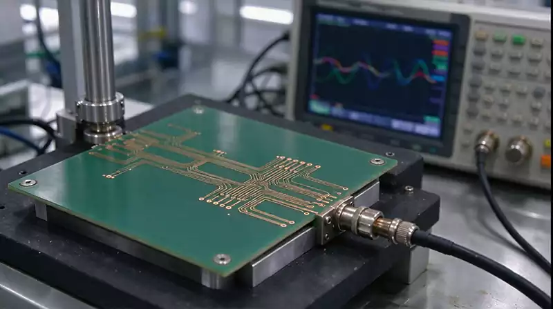
Whenever possible, electrical testing should be performed on representative PCB structures. Impedance testing and insertion loss measurements can be used to compare different copper foil options under the same substrate, copper thickness, and trace design conditions. Keeping the test conditions consistent makes it easier to identify whether performance differences come from the copper foil, dielectric material, or manufacturing process.
Choosing Between RA Copper and ED Copper for PTFE High-Frequency PCBs
RA copper and ED copper each have their own advantages and suitable applications. RA copper generally offers good ductility and a relatively smooth surface, making it worth considering for low-loss high-frequency designs and applications that require better bending performance. ED copper is available in a wide range of specifications, and its surface profile can be adjusted through different treatments. Low-profile VLP and HVLP products are also suitable for many high-frequency circuits. For projects that place greater emphasis on established manufacturing processes and production cost, ED copper can be a practical choice.
The right copper foil for a PTFE high-frequency PCB ultimately depends on the operating frequency, loss budget, bonding requirements, and manufacturing conditions. If conductor loss is a major concern, engineers can compare the actual roughness and transmission performance of RA and HVLP copper. If the project places greater emphasis on production scale, process maturity, and cost, suitable ED copper grades should also be evaluated. In either case, the decision should be supported by product specifications and test results rather than assumptions based on the foil category.
For PCB manufacturers, understanding the customer’s operating frequency, allowable insertion loss, and reliability requirements is usually more useful than recommending one copper foil type by default. Evaluating copper foil specifications, PTFE laminate construction, and actual manufacturing capabilities together helps reduce the gap between material selection and production performance.
Frequently Asked Questions
What is the main difference between RA copper and ED copper?
The main difference is their manufacturing process. RA copper is produced through mechanical rolling and annealing, which generally gives it good ductility and a relatively smooth surface. ED copper is produced through electrochemical deposition, and its surface profile can be adjusted through subsequent treatments. Their high-frequency performance, flexibility, and bonding characteristics may differ depending on the specific foil grade and application.
Why is RA copper often considered for PTFE high-frequency PCBs?
RA copper generally offers low surface roughness, which can help reduce the influence of surface irregularities on high-frequency current flow. This makes it worth considering for microwave and millimeter-wave low-loss circuits. RA copper also generally offers good ductility. However, its suitability for a PTFE laminate still depends on the surface treatment and the resulting bond strength.
Can ED copper be used in PTFE high-frequency PCBs?
Yes. ED copper is not limited to conventional PCB applications. VLP and HVLP copper foils are specifically designed to provide controlled surface profiles for high-frequency applications. Many PTFE circuit designs can use these products successfully. Selection should be based on the actual roughness, peel strength, and electrical performance data rather than the ED classification alone.
Does RA copper always have lower high-frequency loss than ED copper?
No. RA copper generally has a smoother surface, but ED copper grades can also vary considerably in surface roughness. Low-profile ED copper, in particular, may deliver high-frequency performance comparable to some RA products. A meaningful comparison requires consistent copper thickness, dielectric material, trace geometry, and test frequency.
Why is copper adhesion difficult to control on PTFE laminates?
PTFE has low surface energy and high chemical inertness, making it difficult to form a strong bond with copper foil. Manufacturers generally need suitable copper surface treatments, bonding systems, or specialized lamination processes to improve adhesion. The final peel strength also depends on the material formulation and processing conditions.
Which copper foil surface roughness should be checked for high-frequency applications?
For PTFE copper-clad laminates, particular attention should be paid to the copper surface that contacts the dielectric. Its microscopic profile can influence both high-frequency current transmission and interfacial bonding. When reviewing supplier data, confirm which side is being measured and whether the reported parameter is Ra, Rz, RMS, or another measurement.
Is RA copper always more expensive than ED copper?
Not necessarily. Copper foil pricing depends on thickness, surface treatment, product grade, supplier, and order volume. Some RA products may cost more, but the actual difference should be confirmed through supplier quotations. The evaluation should also consider how the selected foil affects electrical performance and manufacturing yield.
Should 77 GHz automotive radar PCBs use RA copper or ED copper?
At 77 GHz, copper surface roughness deserves careful evaluation because it can influence conductor loss at millimeter-wave frequencies. RA copper is one option worth considering, while HVLP ED copper should also be included in the comparison. The final decision should take into account the PTFE laminate construction, insertion loss requirements, peel strength, and measured performance.
Is RA copper suitable for every PTFE PCB?
No. RA copper is worth considering for designs with demanding low-loss or ductility requirements, but it is not necessarily the best option for every PTFE PCB. For applications with less stringent loss requirements and greater emphasis on production scale and cost, an ED copper foil that meets the design specifications may be equally suitable.
How can manufacturers verify the performance difference between RA and ED copper?
A practical approach is to produce comparison test coupons using the same PTFE material, copper thickness, and trace design. The samples can then be evaluated through impedance testing, insertion loss measurements, and copper peel strength testing. For applications with demanding reliability requirements, thermal cycling and relevant process validation should also be considered. Consistent test conditions are essential for determining whether either copper foil meets the product requirements.