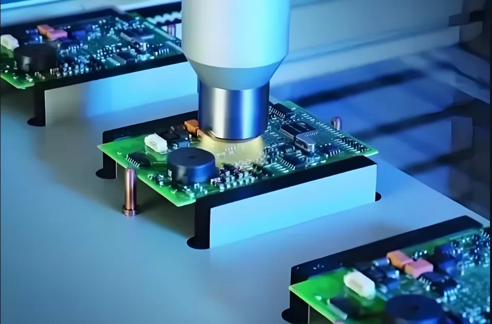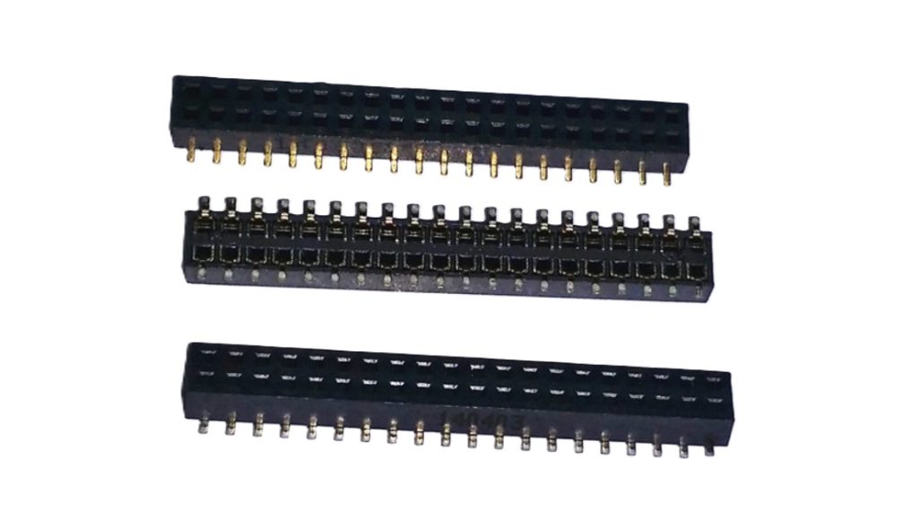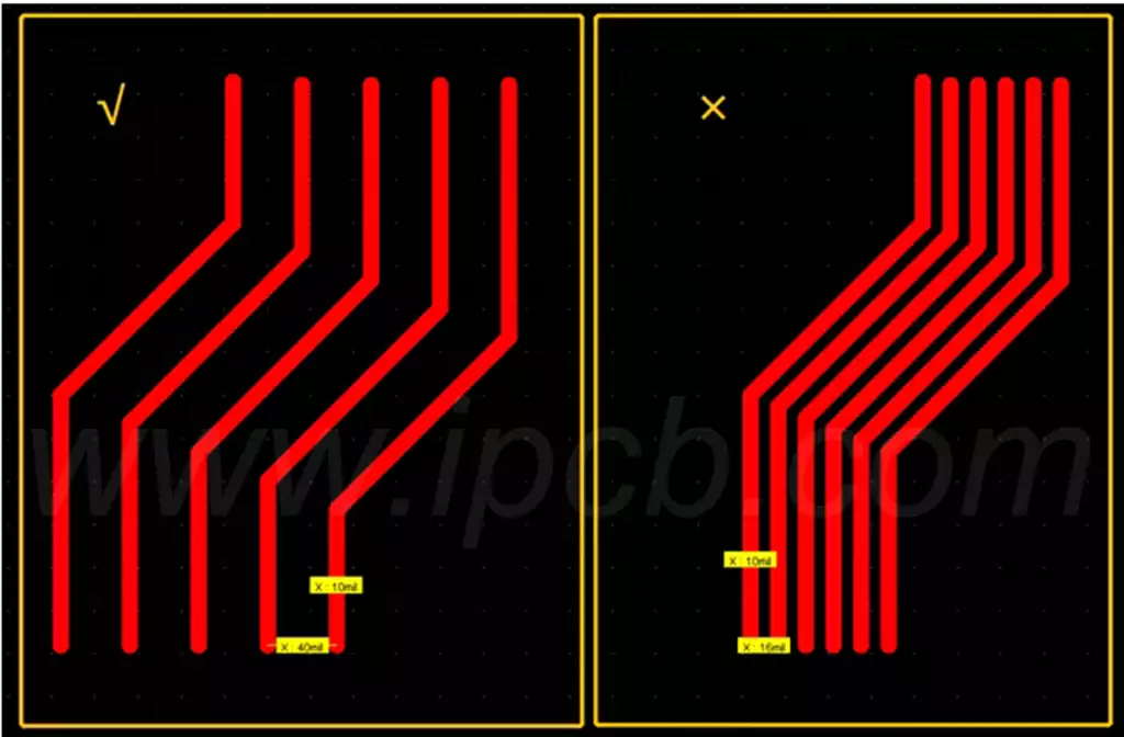
Copper voids in PCB through holes are plating defects that occur when copper does not form a continuous conductive layer along the drilled hole wall. These defects can appear as small unplated areas, gaps in the copper deposit, or larger regions where the hole wall has insufficient copper coverage. Because plated through holes provide electrical connections between different PCB layers, even a small void can affect electrical continuity and long term reliability.
Understanding what causes copper voids in PCB through holes is essential for PCB designers, manufacturing engineers, and quality control teams. Although the defect is often discovered during electrical testing or microsection inspection, its underlying causes usually originate much earlier in the manufacturing process. Drilling quality, hole cleaning, desmear, chemical copper deposition, electroplating, and process control can all influence the final condition of the plated hole wall.
What Are Copper Voids in PCB Through Holes
A plated through hole is created by drilling a hole through the PCB laminate and depositing a conductive copper layer on its inner wall. This copper layer connects copper pads and internal circuit layers, allowing electrical signals and power to pass through the board.
Copper voids occur when the deposited copper layer is discontinuous or locally missing. Instead of forming a uniform conductive coating, the plating process leaves an area with inadequate copper coverage or no copper at all.
The size and location of a void influence its potential impact. A small isolated defect may not immediately cause an open circuit, but it can reduce the effective copper cross section and create a weak point. Larger voids can interrupt electrical continuity, while defects extending through multiple regions of the hole wall may cause serious reliability problems.
Copper voids should also be distinguished from other through hole plating defects. Thin copper plating means that copper is present but its thickness is below the required specification. A copper void refers to a discontinuity or missing deposit. Copper cracks, by comparison, are fractures in an initially deposited or subsequently stressed copper layer. These defects can have different root causes and require different corrective actions.
Main Causes of Copper Voids in PCB Through Holes
Copper voids rarely result from a single manufacturing factor. In many cases, several process conditions combine to prevent proper copper deposition on the hole wall.
Poor Drilling Quality and Hole Wall Damage
Mechanical drilling is one of the earliest processes that affects through hole plating quality. During drilling, the cutting action of the drill bit can generate heat, mechanical stress, resin smear, and debris along the hole wall.
If drilling parameters are unsuitable, the hole wall may develop rough areas, excessive resin smear, or damaged glass fibers. These conditions can interfere with subsequent cleaning and metallization processes.
Resin smear is particularly important because it can cover exposed copper at internal layer connections. If the smear is not adequately removed, the chemical copper process may not establish reliable electrical contact with the internal copper layers. This can result in plating discontinuities or poor connections around the hole wall.
Worn drill bits, incorrect feed rates, unsuitable spindle speeds, and inadequate drilling conditions can increase the risk of hole wall damage. Therefore, controlling drill quality and replacing tools at appropriate intervals are important steps in preventing plating defects.
Inadequate Desmear and Hole Cleaning
After drilling, the hole walls must be cleaned and prepared before copper deposition. Desmear removes resin residue produced during drilling and exposes the underlying copper and glass reinforcement needed for reliable metallization.
If desmear is insufficient, residual resin can remain on the hole wall and prevent the chemical copper layer from forming continuously. This is especially problematic around internal copper connections, where resin contamination may block the electrical contact between the deposited copper and the internal copper layers.
However, excessive desmear can also create problems. Over processing may damage the laminate, expose or weaken glass fibers, and produce an uneven hole wall surface. Such conditions can make subsequent chemical treatment and copper deposition less consistent.
The desmear process must therefore be matched to the laminate material, board construction, and drilling conditions. Effective control requires more than simply increasing treatment time or chemical concentration.
Poor Electroless Copper Deposition
Electroless copper plating is a critical stage in through hole metallization. Before electroplating can take place, a thin conductive copper layer must be deposited on the nonconductive hole wall.
This initial copper layer provides the electrical path required for subsequent electrolytic copper plating. If electroless copper deposition is incomplete, the electroplating process may not be able to build copper in the affected areas.
Several factors can cause poor electroless copper coverage. Inadequate conditioning, poor catalyst adsorption, unstable chemical concentrations, contamination, unsuitable bath temperature, and insufficient reaction time can all affect deposition quality.
If the hole wall is not properly activated, the chemical copper reaction may not start uniformly. Some areas may receive sufficient copper while others remain poorly covered or completely unplated. These areas can later appear as copper voids in microsection inspection.
For this reason, chemical copper deposition must be controlled carefully, particularly when manufacturing multilayer, high aspect ratio, and high density interconnect PCBs.
Inadequate Electroplating and Poor Solution Distribution
After electroless copper deposition, electroplating increases the copper thickness on the hole wall to meet the required manufacturing specification.
Poor electroplating conditions can lead to uneven copper distribution, insufficient thickness, and localized plating defects. Although inadequate electroplating does not always create a complete void, it can expose weaknesses in the initial conductive layer and increase the risk of discontinuous copper coverage.
The distribution of plating solution inside the holes is particularly important. In high aspect ratio PCBs, the hole diameter is relatively small compared with the board thickness. This makes it more difficult for fresh plating solution to reach the center of the hole and for reaction by products and gas bubbles to be removed.
If solution exchange is insufficient, copper deposition may become uneven along the hole wall. The center of a deep hole may receive less effective plating than the areas near the surface.
Poor agitation, unsuitable current density, incorrect plating time, and inadequate bath control can further contribute to this problem. Manufacturing engineers must optimize these parameters according to the board thickness, hole diameter, copper distribution requirements, and plating chemistry.
Air Bubbles Trapped Inside Through Holes
Air bubbles trapped inside through holes can prevent plating solution from contacting parts of the hole wall. When a bubble remains attached to the surface during chemical or electrolytic copper deposition, the covered area may not receive the required copper deposit.
This can result in localized unplated regions that appear as voids during inspection.
The risk is higher when through holes have a high aspect ratio or when wetting and solution circulation are inadequate. Small diameter holes can make it more difficult for liquids to enter and displace trapped air, particularly when the PCB enters a treatment bath without sufficient wetting or agitation.
Proper pre wetting, solution movement, and process design help reduce this risk. Operators should also monitor whether the equipment provides adequate circulation and whether the treatment sequence allows trapped air to escape before metallization begins.
Chemical Bath Contamination and Process Instability
Chemical copper and electroplating solutions must remain within their specified operating ranges. Contamination or unstable chemical conditions can affect reaction rates, deposition uniformity, and the adhesion of the copper layer.
Metallic impurities, organic contamination, excessive reaction by products, and incorrect concentrations can all reduce plating performance. Changes in temperature, pH, or other chemistry specific control parameters may also cause inconsistent deposition.
When the chemical copper bath becomes unstable, the initial conductive layer may develop weak or incomplete coverage. If the electroplating bath is poorly controlled, copper thickness and distribution may also become inconsistent.
Regular chemical analysis, filtration, bath maintenance, and process monitoring are therefore essential. Simply extending plating time cannot reliably compensate for an unstable chemical process.
High Aspect Ratio and Difficult Through Hole Geometry
PCB thickness and hole diameter have a direct influence on through hole plating difficulty. A high aspect ratio hole has a relatively large depth compared with its diameter, making it more challenging to maintain uniform chemical exchange and copper deposition throughout the hole.
As the aspect ratio increases, plating solution must travel farther into a narrow opening. This can reduce solution exchange in the center of the hole and make it more difficult to remove bubbles and reaction by products.
The result may be uneven copper thickness, poor coverage, or localized void formation. These challenges become more significant in thick multilayer boards, small diameter through holes, and designs with demanding plating requirements.
PCB manufacturers must consider aspect ratio during process planning rather than treating all through holes as equivalent. Hole diameter, board thickness, plating chemistry, agitation, and current distribution should be evaluated together.
How Copper Voids Affect PCB Reliability
Copper voids can influence both the electrical performance and mechanical reliability of a PCB. The severity depends on the size, location, distribution, and continuity of the defect.
Electrical Continuity Problems
The primary function of plated through holes is to provide electrical connections between different layers. When copper coverage is interrupted, the conductive path may become unstable or completely open.
A large void can prevent current from passing through the hole. Smaller defects may leave enough copper for initial electrical continuity but reduce the available conductive cross section. This can increase resistance and create localized heating under certain operating conditions.
In multilayer boards, unreliable connections can affect signal transmission, power distribution, and the overall functionality of the electronic assembly.
Reduced Mechanical Strength
The copper barrel inside a through hole also contributes to the mechanical integrity of the connection. Inadequate copper coverage reduces the effective plated area and may create localized weak points.
During thermal cycling, the PCB laminate and copper experience different levels of expansion and contraction. If the copper layer already contains defects, repeated thermal stress can increase the likelihood of cracking or connection failure.
This is particularly important in applications exposed to temperature fluctuations, vibration, or demanding operating environments.
Long Term Reliability Risks
A PCB with copper voids may pass an initial electrical test but still experience failures during service. Small defects can become more significant when exposed to repeated thermal cycling, current loading, and mechanical stress.
For products used in automotive electronics, industrial control systems, power electronics, and other reliability sensitive applications, through hole plating quality is therefore an important manufacturing consideration.
Preventing copper voids is more effective than relying only on final electrical testing to identify defective boards.
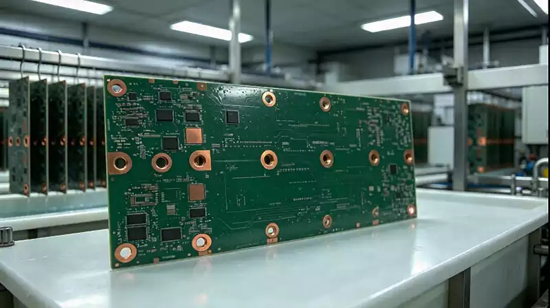
How to Detect Copper Voids in PCB Through Holes
Copper voids are not always visible from the PCB surface. Since the defect is located inside the plated hole, specialized inspection methods are needed to evaluate the condition of the copper barrel.
Microsection Analysis
Microsection analysis is one of the most widely used methods for examining through hole plating quality. A PCB sample is cut through the plated hole, mounted, ground, polished, and examined under a microscope.
The cross section allows inspectors to evaluate copper thickness, hole wall coverage, internal layer connections, and the presence of voids or cracks.
Microsection inspection is particularly useful for identifying defects that are difficult to detect through external visual inspection. It also helps manufacturing engineers determine whether the problem originates from incomplete initial metallization, uneven electroplating, or other process conditions.
Electrical Continuity Testing
Electrical testing checks whether the required connections between PCB layers are electrically continuous. A through hole with a complete copper break may be identified as an open circuit.
However, electrical testing cannot always identify small voids that do not immediately interrupt the conductive path. A board may pass continuity testing even when its plated copper contains localized defects.
For this reason, electrical testing should be combined with appropriate structural inspection and process monitoring.
Reliability Testing
Thermal stress and thermal cycling tests can help evaluate whether plated through hole connections remain reliable under temperature changes.
These tests are particularly useful when assessing the impact of plating defects on long term performance. They can reveal weaknesses that may not be apparent during initial electrical inspection.
The appropriate test method and acceptance criteria depend on the PCB specification, product requirements, and applicable industry standards.
How to Prevent Copper Voids in PCB Through Holes
Preventing copper voids requires coordinated control across drilling, hole preparation, chemical copper deposition, and electroplating. Focusing on only one process stage may not eliminate the underlying problem.
Optimize Drilling Parameters
PCB manufacturers should select drilling conditions according to the laminate material, board thickness, hole diameter, and drill bit characteristics. Feed rate, spindle speed, tool wear, and drilling sequence should be monitored to reduce resin smear and hole wall damage.
Regular drill bit inspection and replacement are also important. Worn tools can produce rougher hole walls and increase the burden on downstream cleaning processes.
Improve Desmear and Hole Preparation
The desmear process should remove drilling residue without excessively damaging the laminate or glass reinforcement. Chemical concentration, temperature, treatment time, and process sequence should be controlled according to the material system.
Hole cleaning and conditioning must also ensure that the surface is suitable for catalyst adsorption and subsequent chemical copper deposition.
A well prepared hole wall provides a more reliable foundation for continuous metallization.
Maintain Stable Electroless Copper Chemistry
The electroless copper process must create a continuous conductive layer throughout the hole. Manufacturers should monitor bath composition, temperature, pH where applicable, treatment time, and contamination levels according to the chemistry supplier’s specifications.
Proper conditioning and activation are equally important because poor catalyst coverage can result in incomplete copper deposition.
Regular bath analysis and maintenance help maintain consistent plating performance across production batches.
Optimize Electroplating Conditions
Electroplating parameters should be adjusted to achieve uniform copper distribution throughout the hole. Current density, plating time, solution circulation, temperature, and chemical composition must be controlled as part of a coordinated process.
For high aspect ratio boards, manufacturers may need plating processes and equipment specifically designed to improve solution exchange and copper distribution inside narrow holes.
The goal is not simply to increase the total copper thickness but to achieve reliable and consistent coverage along the entire hole wall.
Improve Wetting and Solution Circulation
Effective wetting helps plating solutions enter through holes and contact the complete hole wall. Appropriate pre treatment, agitation, and solution circulation reduce the possibility of trapped air and improve chemical exchange.
This is particularly important for small diameter and high aspect ratio holes, where liquid movement is more restricted.
Manufacturers should evaluate whether their process equipment provides sufficient circulation for the actual PCB construction and hole geometry being produced.
Strengthen Process Inspection and Statistical Control
Copper void prevention should be supported by routine inspection and process data analysis. Microsection samples can be used to verify hole wall coverage and copper thickness, while electrical testing provides additional information about connection continuity.
When defects occur, engineers should trace them back through the relevant production stages rather than adjusting plating parameters without identifying the root cause.
Recording defect location, hole geometry, drilling conditions, chemical bath status, and plating parameters can help identify recurring patterns. Statistical process control can then be used to detect process variation before it results in a larger number of defective boards.
Copper Voids in High Density and Multilayer PCBs
Copper void prevention becomes more challenging as PCB designs become thinner, denser, and more complex.
Multilayer PCBs often contain many plated through holes connecting multiple copper layers. These holes must maintain reliable electrical connections despite variations in board thickness, material properties, and drilling conditions.
High density interconnect designs may also use smaller holes and more demanding aspect ratios. As hole dimensions decrease, cleaning, wetting, chemical activation, and solution circulation become more difficult to control.
For manufacturers producing multilayer and HDI PCBs, process capability should therefore be evaluated against the actual hole geometry and construction requirements. A process that performs well on a standard two layer board may not provide equivalent results on a thick multilayer PCB with small diameter through holes.
Early communication between the PCB designer and manufacturer can help identify potential manufacturing risks. Hole diameter, board thickness, layer structure, copper thickness requirements, and reliability expectations should all be considered during design review.
Common Misunderstandings About PCB Copper Voids
One common misunderstanding is that increasing electroplating time will eliminate all copper voids. This is not necessarily true. If the hole wall has not been properly cleaned, activated, or covered with electroless copper, additional electroplating time may not restore the missing conductive layer.
Another misconception is that a PCB without electrical open circuits has no through hole plating defects. Electrical testing can identify many continuity failures, but it does not necessarily reveal small voids or areas of insufficient copper thickness. Structural inspection remains important when evaluating plating quality.
It is also incorrect to assume that all copper voids originate in the electroplating stage. Drilling, desmear, conditioning, activation, and chemical copper deposition can all contribute to incomplete hole wall coverage. Effective corrective action requires identifying the actual process stage responsible for the defect.
Frequently Asked Questions About Copper Voids in PCB Through Holes
What is the main cause of copper voids in PCB through holes?
There is no single universal cause. Common contributing factors include poor drilling quality, inadequate desmear, incomplete hole wall activation, poor electroless copper deposition, trapped air bubbles, and unstable electroplating conditions. The specific root cause must be identified through process investigation and microsection analysis.
Can copper voids cause PCB failure?
Yes. Copper voids can interrupt electrical continuity, increase resistance, reduce the effective copper cross section, and weaken plated through hole connections. Even when a small defect does not cause an immediate failure, it may reduce long term reliability under thermal and mechanical stress.
How are copper voids detected in PCB through holes?
Microsection analysis is a common method because it allows inspectors to examine the internal copper layer directly. Electrical continuity testing can identify open connections, while thermal stress and reliability testing help evaluate the durability of plated through hole connections.
What is the difference between a copper void and thin copper plating?
A copper void is an area where the copper deposit is discontinuous or missing. Thin copper plating means that copper is present but does not meet the required thickness. Both conditions can affect reliability, but they represent different types of plating defects.
Are high aspect ratio holes more likely to develop copper voids?
High aspect ratio holes present greater plating challenges because their narrow geometry makes it harder for treatment solutions to circulate and exchange throughout the hole. If wetting, chemical activation, or plating conditions are inadequate, incomplete coverage and copper voids may occur.
Can copper voids be prevented completely?
Manufacturing controls can significantly reduce the risk, but prevention depends on the PCB construction, hole geometry, material system, and process capability. Consistent drilling, effective desmear, stable chemical copper deposition, optimized electroplating, and routine inspection are essential for maintaining reliable through hole plating quality.
Copper voids in PCB through holes are important manufacturing defects because they can compromise electrical connections and reduce the long term reliability of a printed circuit board. Their causes may originate in drilling, desmear, hole preparation, electroless copper deposition, or electroplating, making a complete process review necessary when defects are discovered.