PCB copy board, also known as circuit board cloning, is to copy the circuit board to be copied, is a process from the physical to the PCB, that is, a ready-made PCB board into a PCB for mass production.
PCB copy board is a kind of reverse research technology, that is, through a series of reverse research techniques to obtain an excellent electronic product PCB design circuit, and circuit schematic and BOM table. Through this reverse research method, other people need two or three years to develop a product, we through the PCB copy board reverse research method, it may only take a month to learn other people spend two or three years to research and development out of the results, which for our developing countries to catch up with the world’s footsteps has played a very important role in promoting. And the development of reverse research technology, but also for those development team technology breakthroughs play a role in promoting the development of reverse research technology at the same time also lead to the continuous updating of the forward research technology. Positive research and reverse research is because of this competitive relationship between the development of electronic technology in the past few years in order to rapidly changing, electronic products, almost a year of replacement, behind the electronic products will only be updated faster and faster. Because PCB copy board lowers the threshold of electronic technology, PCB copy board makes more and more developing countries quickly embarked on the forefront of high-tech electronic technology, and developed countries together with the research of electronic technology. The larger the research team, the faster the world’s electronic technology can develop.
How to copy a pcb board
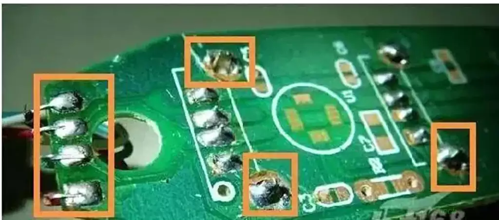
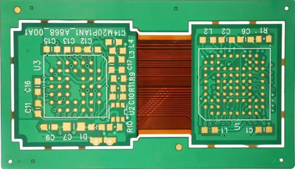
- Take a PCB board, first of all, you need to record on paper all the components of the model, parameters and location, especially diodes, tertiary direction, the direction of the IC gap. It is best to use a digital camera to take two photos of the location of the components.
- Remove all components, to remove the tin in the PAD hole. Use alcohol to scrub the board clean, and then put it into the scanner, when scanning in the scanner to slightly adjust the scanning pixels, to get a clearer image of the board. Then use water gauze paper to lightly sand the top and bottom layers, sanding until the copper film shiny, into the scanner, start PHOTOSHOP, with color way to scan the two layers respectively. Note that the PCB board must be placed in the scanner within the horizontal and vertical, otherwise the scanned image can not be used.
- Adjust the contrast of the canvas, brightness and darkness, so that there is a strong contrast between the part of the copper film and the part of the copper film does not form a strong contrast, and then turn the picture to black and white, check whether the lines are clear, if not clear, we must continue to adjust. If clear, the map will be saved as black and white BMP format two files, if you find that the graphics have problems, but also need to use PHOTOSHOP for correction.
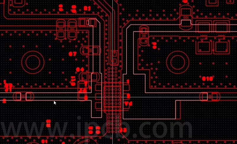
- The two BMP format files were converted to PROTEL format files, in PROTEL into two layers, if the two layers of PAD and VIA location of the basic coincidence, indicating that the first few steps to do a good job, if there is a bias, then repeat the third step, until it coincides with so far, will be converted to the TOP layer of BMP TOP.PCB, pay attention to the transformation to the SILK layer, that is, yellow! PCB, pay attention to convert to the SILK layer, that is the yellow layer, and then you trace the line in the TOP layer is, and according to the second step of the drawing to place the device. After drawing the SILK layer will be deleted, and repeat to know all the layers drawn.
- In PROTEL will be TOP.PCB and BOT.PCB into the transfer, combined into a map on the OK. With a laser printer will be TOP LAYER, BOTTOM LAYER were printed on a transparent film (1:1 ratio), the film to the PCB, compare whether there is a mistake, if not, even if successful.
PCB copy board precautions
Copy board company
Before copying the circuit board, be sure to file the original sample, which is a systematic work, any negligence of the previous process may affect the success of the subsequent project.
If customers need to make a component BOM list while copying the board, they must follow the relevant standards when setting up the components of the PCB file, in order to avoid errors when making the BOM list.
When dismantling the board, information such as the polarity and direction of the components need to be recorded carefully, otherwise errors may occur when restoring the board to make a prototype.
The size of the original PCB board needs to be measured accurately, because the performance of the scanner is different, the scanned board picture may differ in size from the real thing. Make sure the image is the same size as the real thing, otherwise it may lead to the production of the board can not be used and the file is invalid.
The scanned image should be as clear as possible, set the resolution of the scanner to a high level in order to zoom in to view the detailed parts of the PCB board.
For Customers
The PCB provided must be in good condition, if there is any damage, it may not be successfully copied or greatly increase the difficulty of copying the board.
Explain in detail the specific requirements of the copy board, including whether it is necessary to make a BOM list and prototype.
If possible, please provide more information about the PCB to be copied, which will help the copying company to shorten the copying time and improve the success rate.
When sending the original board, please make sure that the package is firm to prevent damage during transportation.
As a key technology in the field of electronic technology, the PCB copy board process, though seemingly simple, actually requires meticulous operation and rich experience. From recording component information to scanning the image, to converting the format and checking the comparison, each step needs to be treated rigorously.