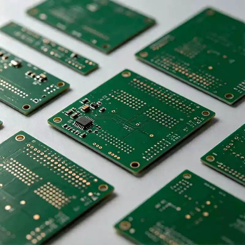
A small circuit board saves space inside a product, but reducing board dimensions does not reduce the number of electrical functions in the same proportion. Power conversion, signal processing, wireless communication, sensing and external connections may still need to fit into an area only a fraction of the original size. The real manufacturing challenge is therefore not simply making the PCB smaller. A reliable small circuit board must preserve electrical isolation, solder-joint quality, thermal control and test coverage while the available space between components continues to decrease.
Board Area Disappears Faster Than Functionality
Connectors, mounting holes, antennas and safety clearances cannot always shrink with the rest of the circuit. After these fixed areas are reserved, the usable routing space may be considerably smaller than the physical outline suggests. This forces components closer together and reduces the number of direct routing channels. The result is a compact PCB in which placement, stack-up and interconnection technology must be considered as one system. Moving one component may affect several traces, the return-current path and the thermal behaviour of nearby devices. For this reason, the manufacturability of a small circuit board should be evaluated before the component layout is frozen. Waiting until Gerber data is released often leaves the manufacturer with very limited options for correcting density-related risks.
Higher Routing Density Changes the PCB Structure
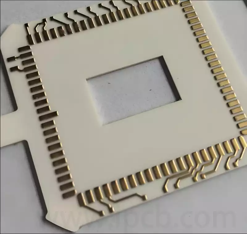
On a conventional PCB, through-holes can connect all copper layers. These holes consume routing space on every layer, even when the electrical connection is only needed between two adjacent layers. As component pitch decreases, conventional through-holes may block the escape paths required beneath fine-pitch packages. A small circuit board may therefore require blind microvias, buried vias, via-in-pad structures or sequential lamination. Microvias can connect selected layers without occupying the full board thickness, allowing more traces to escape from a BGA or another high-I/O package. HDI technology is commonly used for this purpose because it increases interconnection density within a limited area. Würth Elektronik similarly identifies HDI microvia technology as a method of increasing wiring density for miniaturised products.
However, adding HDI features is not automatically the correct solution. The stack-up must match the required connections, trace geometry and manufacturing capability. Unnecessary build-up layers increase cost and introduce additional lamination, drilling and plating operations. Fine traces create another manufacturing constraint. Small variations in imaging, etching or copper plating represent a greater percentage of the finished conductor width. The fabrication data for a small circuit board must therefore specify realistic trace dimensions, annular rings and impedance tolerances instead of relying only on the smallest values shown in a supplier capability table. IPC’s DFM framework draws requirements from standards covering generic PCB design, HDI structures, current-carrying capacity, rigid-board performance, land patterns and soldered assemblies. This reflects why compact-board manufacturability cannot be judged from a single minimum-spacing value. IPC Design for Manufacturing
Assembly Tolerance Becomes a System Problem
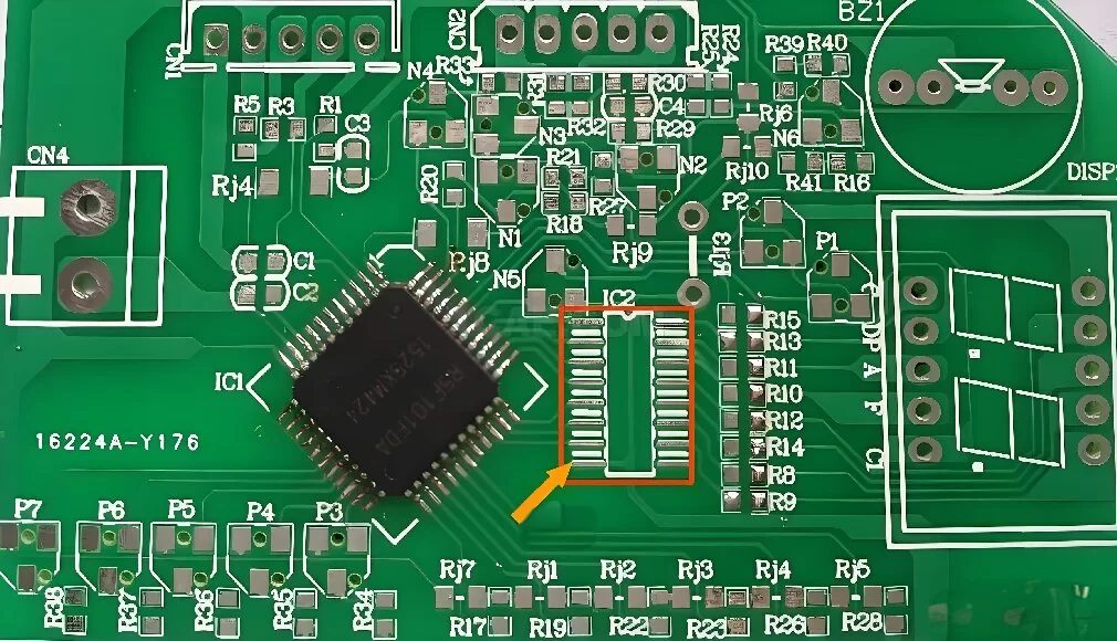
Miniaturisation also narrows the SMT process window. Smaller pads receive smaller solder-paste deposits, so stencil thickness, aperture geometry and paste release become increasingly important. Too little paste may produce an open joint, while excessive or uneven paste can create bridging or component movement during reflow. On a densely populated small circuit board, these defects are not controlled by the stencil alone. Pad design, solder-mask registration, paste characteristics, placement accuracy and reflow behaviour interact with one another. A change intended to correct one defect can introduce another if the complete process is not reviewed. Solder paste inspection should verify deposit volume and alignment before placement. After reflow, automatic optical inspection can detect visible defects, but joints beneath BGA, LGA and other bottom-terminated packages require X-ray inspection. Process limits and acceptance criteria should also be agreed between the product owner and assembler. IPC identifies J-STD-001 as the standard covering requirements for soldered assemblies and IPC-A-610 as the post-assembly acceptance standard. IPC assembly standards
Component orientation matters as well. Large thermal masses positioned close to very small passive components can create uneven heating. Tall connectors can restrict inspection angles, and components placed too close to the edge may interfere with panel rails or depanelisation tools. Reliable fine pitch PCB assembly therefore depends on coordinated placement and process planning rather than placement density alone.
Heat Has Less Space to Spread
A smaller outline does not necessarily mean lower power consumption. When regulators, processors, wireless devices and power transistors are positioned close together, their thermal fields can overlap. This may raise the temperature of nearby capacitors, oscillators or sensors even when each individual component remains within its rated power. Effective PCB thermal management for a small circuit board uses copper planes, thermal vias and appropriate component spacing to move heat away from concentrated sources. Heat-transfer paths must continue through the enclosure or mounting structure; spreading heat across the PCB is of limited value if that heat becomes trapped inside a sealed housing. Texas Instruments notes that junction-to-ambient thermal resistance can depend heavily on PCB layout factors, including the available copper and ground-plane arrangement. Texas Instruments board layout thermal guide
Thermal analysis should consequently use the assembled product’s operating condition rather than room-temperature bench testing alone. Maximum load, enclosure temperature and adjacent heat sources may reveal interactions that are not visible during a short functional test.
Electrical Separation Also Becomes More Difficult
Switching regulators, high-speed digital interfaces, RF circuits and low-level analogue signals can occupy neighbouring areas. Short physical distances increase the risk of switching noise entering a sensor input or radio receiver. The layout of a small circuit board must preserve continuous return paths and keep high-current loops compact. Decoupling capacitors need short connections to the relevant power and ground pins, while antenna keep-out regions must remain clear of copper and components. These areas should not be sacrificed merely to create room for one more device.
Test Access Must Be Planned Early
Test pads are often removed first when board space becomes limited. This saves area during layout but can make programming, fault isolation and production testing considerably harder. A practical small circuit board retains access to essential power rails, ground, reset, communication interfaces and programming signals. Where conventional probe pads cannot be accommodated, the test strategy may combine smaller accessible targets, edge contacts, boundary scan and a dedicated functional fixture. At iPCB, DFM and DFT review can be performed before production to check whether dense layouts can be fabricated, assembled, inspected and tested with repeatable processes. This review is particularly valuable before an HDI stack-up or production fixture has been committed.
Small Boards Still Need Production Handling Space
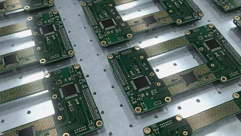
Very small PCBs are rarely processed individually through an SMT line. They are normally placed in a panel with tooling rails, fiducials and support features. The panel must remain sufficiently rigid during printing, placement and reflow. Component clearance from routed edges, V-cuts or breakaway tabs must also be checked. Mechanical stress during depanelisation can damage nearby ceramic capacitors or fine solder joints. Panel design is therefore part of the manufacturing plan for a small circuit board rather than a separate purchasing detail.
Reliability Comes From Coordinating the Whole Process
Miniaturisation is successful when PCB fabrication, component placement, soldering, thermal control, inspection and testing are developed together. A dense layout that can technically be fabricated may still be unsuitable for stable assembly or economical production testing. The most reliable small circuit board is not necessarily the design using the smallest possible trace, via and component spacing. It is the design that uses miniaturisation only where required and leaves sufficient process margin for consistent production. Early DFM review, a realistic HDI stack-up and a defined inspection and testing strategy allow a small circuit board to remain compact without turning every production batch into a yield experiment.