PCB soldering precautions
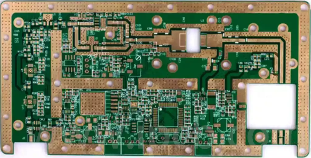
1.EDA365 electronic community suggests that the first task after obtaining the PCB bare board is to carry out visual inspection to confirm that there are no short circuits, broken circuits and other defects, and in-depth understanding of the development board schematic, and PCB screen printing layer carefully compared to ensure that the two are consistent, to prevent the schematic and PCB mismatch.
- In the PCB soldring, to ensure that all the required materials are ready, should be classified and organised components, based on their size into a number of categories, in order to facilitate the welding work in an orderly manner. At the same time, print a detailed list of materials, and in the welding process, each completed a welding task, on the list of the corresponding items to mark the deletion, which helps to track the progress of welding and to ensure that there is no omission.
Before the soldering operation starts, anti-static means such as wearing a static electricity bracelet should be taken to prevent static electricity from causing damage to sensitive components. After ensuring that all the tools and equipment required for welding are ready, it is also necessary to ensure that the soldering iron tip is clean and free of dirt. For beginners, it is recommended to use a flat iron for welding, especially when dealing with small packages such as 0603 and other components, the flat iron can better fit the pads and simplify the pcb soldering process. However, this may not be necessary for experienced solderers.
- When selecting and soldering components, the order from low to high and from small to large should be followed in order to avoid large components that have already been soldered hindering the welding operation of small components. At the same time, integrated circuit chips should be given priority for welding.
- Before soldering an IC chip, it is important to ensure that the chip is placed correctly. The rectangular pads on the silkscreen layer of the chip usually mark the location of the starting pins.PCB soldering process,first fix a pin of the chip, followed by fine-tuning of the chip position, followed by fixing the diagonal of the other pin, to ensure that the chip is in the correct connection position, and then carry out the soldering operation.
5 Chip ceramic capacitors and voltage regulator diodes (in voltage regulator circuits) do not need to distinguish between positive and negative poles,but light emitting diodes, tantalum capacitors,and electrolytic capacitors need to clearly distinguish between positive and negative poles.For capacitors and diode type components,the end with the distinctive marking is usually the negative terminal.In the case of SMD LEDs,the direction of light propagation indicates the flow from positive to negative.For components that are silk screened as diode schematic packages,the end with the vertical line should correspond to the negative terminal of the diode.
- For crystals,passive crystals are usually equipped with two pins, and there is no need to distinguish between positive and negative poles. Active crystals often have four pins, then you need to pay special attention to the specific definition of each pin to ensure that no error when welding.
- For plug-in components, such as power supply module-related components, the pins may need to be properly trimmed before soldering.After the component is properly placed and secured, the soldering iron is usually used to heat up the solder on the backside of the component so that it penetrates from the pads to the front side to complete the soldering. Although the amount of solder used should not be excessive,the first priority is to ensure that the component can be firmly fixed.
- In the soldering operation,once found on the PCB design flaws, such as the installation process of interference phenomena, improperly designed pad size, component package mismatch and other issues, should be immediately recorded for subsequent design and process improvements.
- After soldering should use a magnifying glass to view the solder joints, check whether there is a false weld and short circuit and so on.
10.After the completion of the pcb soldering work,alcohol and other cleaning agents should be used to clean the surface of the circuit board to prevent the circuit board surface attached to the iron filings make the circuit short-circuit, but also to make the pcb board more clean and beautiful.
Soldering methods for double sided pcb
In order to ensure that double sided pcb has reliable conductive properties, EDA365 Electronic Community recommends that you first properly connect the double-sided boards to the via holes (i.e., the through-hole areas that have been metallised) by pcb soldering wires,etc.,and after soldering is complete,trim off the protruding tips on the connecting wires to prevent them from accidentally scratching the operator’s hands.This step is a critical part of the preparation of double sided pcb board connections.
Key steps for double sided pcb soldering:
1.For components that need to be shaped,you must follow the instructions of the process drawings for pre-processing,that is,shaping before plug-in.
2.After shaping the diode type surface should be facing up,and to ensure that its two pins of the same length.
3.When inserting components with polarity requirements,attention must be paid to the direction of polarity, and must not be inserted in reverse. For integrated blocks and other components,after insertion,regardless of whether it is vertical or lying down,there shall be no obvious tilt.
4.Soldering iron power should be used between 25 to 40 watts,the temperature of the iron head should be controlled at about 242 ℃, too high is easy to damage the iron head, too low is unable to melt the solder, pcb soldering time should be controlled between 3 to 4 seconds.
5.Formal soldering,generally should follow the principle of operation from short to high,from the inside to the outside, master the pcb soldering time,so as not to overheat and damage the components or copper-clad lines.
6.In view of the double sided pcb soldering, it is also necessary to create a process frame for placing the pcb board to prevent the following components are pressed oblique.
7.After the completion of pcb soldering,a comprehensive inspection should be carried out to ensure that there is no missing plug-ins and soldering points, to confirm that there is no error,the excess component pins to be trimmed, and then flow into the next process.
8.In actual operation, the relevant process standards must be strictly adhered to, in order to ensure the welding quality of the product.
With the rapid development of science and technology,and people’s daily lives are closely linked to the continuous renewal of electronic products, people’s high-performance,small and portable,multi-functional electronic products of the growing demand,which puts forward the design and manufacture of pcb board a new challenge and requirements.
