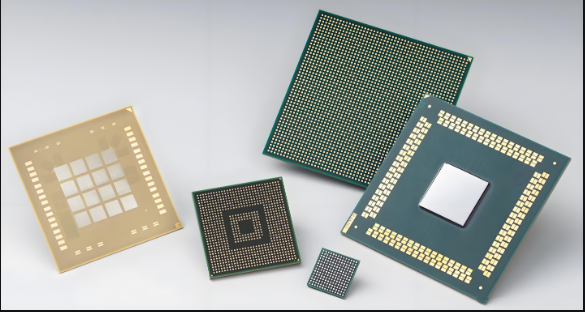
Ceramic PCBs are not merely a simple substitute for FR-4. Thanks to their inherent advantages—such as low thermal expansion, high insulation and high-temperature resistance—they are widely used in demanding applications such as RF communications, automotive electronics and medical equipment.
However, their characteristics of being ‘hard and brittle’ and ‘sensitive to thermal mismatch’ make the SMT process a rigorous test of precision and temperature control. Mastering the soldering of ceramic substrates hinges on a thorough understanding of material properties, a detailed analysis of process critical points, and the establishment of a comprehensive quality control system to eliminate potential issues such as solder balls, tombstoning and substrate cracking at the source.
Core Advantages and Process Challenges of Ceramic PCBs
Advantages: The coefficient of thermal expansion (CTE) is significantly lower than that of FR-4, offering excellent dimensional stability and making it suitable for high-frequency signals and high-density routing; it is heat-resistant and corrosion-resistant, capable of withstanding multiple reflow cycles and harsh environments.
Weaknesses: Hard and brittle, prone to fracturing under mechanical impact; uneven thermal stress can easily cause delamination; solder tends to spread when the surface is not covered by a solder mask, and pad oxidation directly affects wetting.
Therefore, SMT for ceramic PCBs must be centred on ‘precise temperature control, strict stress management, and fine printing’; any oversight at any stage may render all previous efforts futile.
Key Process Flows for Ceramic PCBs
1.Pad and Stencil Design
Pad design adheres to the principle of “small yet precise”:
The aspect ratio of surface-mount component pads should be controlled between 1.2:1 and 1.5:1, with a spacing of ≥0.15 mm;
Thermal isolation design should be implemented for devices such as BGAs and QFNs to reduce thermal stress concentration;
The openings in the solder mask should be 0.05–0.1 mm smaller than the pads to prevent solder overflow.
Stencil design must precisely match the pads:
Material: stainless steel, thickness 0.1–0.15 mm (0.1 mm for 01005/0201 components, 0.15–0.2 mm for BGAs);
Aperture size should be 5%–10% smaller than the pad, with edges polished to Ra < 0.8 μm;
Inverted trapezoidal or concave apertures are used for surface-mount components to prevent excess solder paste; stepped stencils are used for fine-pitch devices.
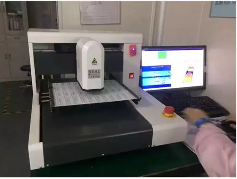
2.Solder Paste Selection and Printing
Solder paste selection:
Prioritise Type 3/4 lead-free solder paste (e.g. SAC305), which has uniform particles and stable activity;
For high-frequency applications, select low-residue, low-volatility flux to avoid affecting insulation;
Store at 0–10°C in a refrigerator; allow to warm up for 4 hours prior to use and stir for 5–10 minutes.
Printing Control:
Fully automatic printers equipped with high-precision vision alignment, with alignment accuracy ≤±0.02 mm;
Squeegee pressure 10–30 N, speed 20–50 mm/s, separation speed 0.5–1 mm/s;
Clean the underside of the stencil every 5–10 boards;
Immediately after printing, use SPI to inspect solder paste volume, misalignment and bridging.
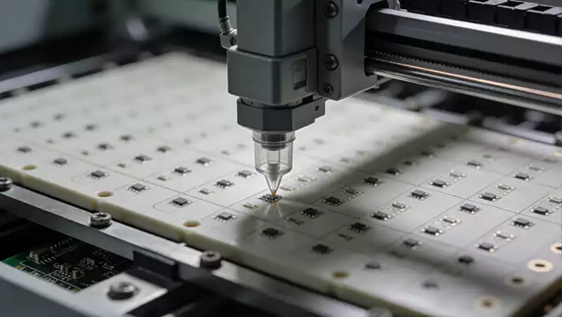
3.Component Placement
Ceramic pcbs are highly rigid and cannot be bent, imposing stringent requirements on placement:
Placement machine repeatability ≤ ±10 μm, supporting vacuum suction and soft gripping;
Placement pressure: small components < 3 N, large components < 5 N, to prevent substrate cracking;
Align using PCB reference marks to compensate for dimensional deviations; for BGAs and QFNs, use ‘centre alignment + edge correction’;
Enter the reflow oven within 2 hours of placement to prevent solder paste from absorbing moisture or drying out.
4.Reflow Soldering
Nitrogen atmosphere is recommended (oxygen content ≤ 500 ppm); the temperature profile should follow a ‘slow ramp-up, thorough preheating, precise peak, rapid cooling’ profile:
| stage | Temperature range | Parameter requirements |
| Preheating zone | Room temperature → 150°C | Heating rate ≤ 1.5 °C/s, duration 60–90 seconds |
| Holding zone | 150–200 °C | Duration: 60–120 seconds |
| Recirculation zone | Peak temperature: 235–245 °C | 20–30 °C above the liquidus, melting in 30–60 seconds |
| Cooling zone | cool to room temperature | Cooling rate ≤ 4 °C/s |
Risk mitigation: Excessively rapid heating may cause thermal shock cracking of the substrate; excessively high peak temperatures or prolonged holding times may result in solder collapse or an excessively thick IMC layer. For each new product, a temperature profile must be determined using a furnace temperature tester.
Common Issues and Solutions
| Defect type | The main reason | Remedial measures |
| Welding balls, erecting a monument | Excessive solder paste, inappropriate stencil aperture size, too rapid preheating, and excessively high peak temperature | Optimise the aperture size of the steel mesh (reduce by 5%–10%) and use SPI to prevent over-printing; preheat at a rate of ≤1.5°C/s; maintain a peak temperature of ≤245°C to reduce the melting time |
| Cracks in the substrate | Excessively rapid heating or cooling, excessive mounting pressure, moisture on the substrate | Control the heating/cooling rate to ≤4°C/s; precisely control the mounting pressure; store in a moisture-proof environment and bake before use |
| Poor soldering, poor wetting | Oxidation of pads, contamination of the solder mask, insufficient solder paste activity, and inadequate reflow temperature | Incoming inspection of pad cleanliness; selection of highly active solder paste; ensuring the peak reflow temperature; nitrogen shielding |
Strategies for Improving Yield
1.Design Optimisation
Pad dimensions comply with the IPC-7351 standard, with a spacing of ≥0.15 mm;
Implement thermal isolation for BGA pads; ensure consistent shrinkage rates across all layers in multilayer ceramic PCBs;
Optimise impedance control for high-frequency applications.
2.Material Control
Ensure solder paste batches are consistent and avoid mixing;
Incoming component inspection must confirm that leads are free from oxidation;
Store ceramic substrates at a humidity of ≤60% RH to prevent moisture absorption.
3.Inspection and Rework
Three-stage inspection: SPI after printing, AOI after reflow, and X-ray for BGA/QFN (void rate ≤ 25%).
Rework guidelines: Use a dedicated ceramic rework station with a heating rate of ≤ 2°C/s; remove old solder first to avoid damaging the pads; match the solder paste and follow the reflow profile when reballing; perform power-on testing after rework.
The SMT process for ceramic PCBs essentially requires a deep understanding of material properties and meticulous control throughout the entire production process. In the future, this process will evolve towards greater precision, intelligence and environmental sustainability.