In the design of power adapters, the quality of the PCB routing on the bare PCB directly determines the stability, reliability and electromagnetic compatibility (EMC) of the entire unit. A well-designed PCB routing not only effectively suppresses noise and reduces losses, but also helps to mitigate safety compliance risks.
Six Key PCB Routing Techniques
1.Current Paths and Loop Control — The Core of Power Circuit Design
Core Principle: The primary focus of PCB routing is on ‘noise loops’ characterised by high di/dt (current rate of change) and high dv/dt (voltage rate of change). Ensuring these loops are as short as possible and enclose the smallest possible area is the fundamental method for suppressing EMI and the core objective of PCB routing optimisation.
Noise loops requiring particular attention:
Input loop: Input capacitor → Switching transistor → Primary winding of the transformer → Back to the negative terminal of the input capacitor. This is the primary source of noise on the primary side; PCB routing must prioritise optimising this loop path.
Output loop: Secondary winding of the transformer → Output rectifier diode → Output capacitor → Back to the secondary winding of the transformer. This directly affects output voltage ripple; PCB routing must ensure the path is compact and free of redundancy.
Practical recommendations (PCB routing techniques):
For the main power paths (especially ground lines), use copper pads instead of fine traces wherever possible. Large copper pads not only have a high current-carrying capacity but also reduce impedance and thermal resistance, minimising losses; they are the preferred solution for high-power PCB routing.
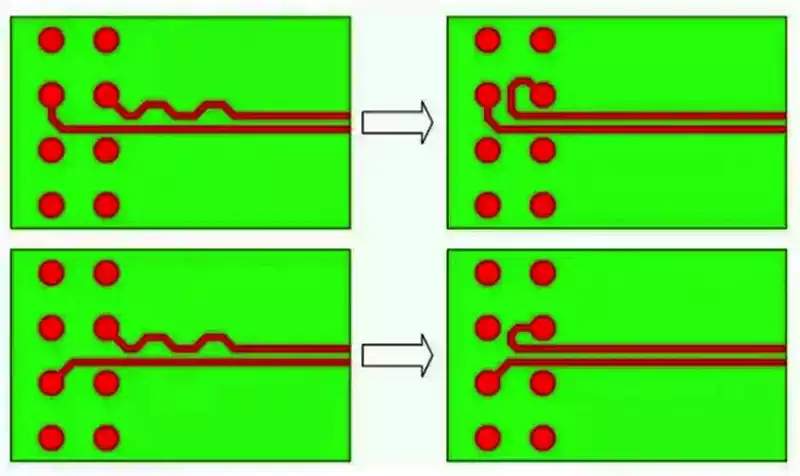
PCB routing should follow the principle of ‘connecting the main trunk first, then branching out’. For example, input electrolytic capacitors and output solid-state capacitors should be directly connected via PCB traces to the start and end points of the noise loop, allowing the pulse current to close within the loop and avoiding interference caused by flowing through the common ground plane.
To illustrate PCB routing techniques using a flyback power supply as an example: the positive and negative terminals of the input capacitor should be connected via the shortest, widest PCB traces (copper traces) to the drain and source terminals of the MOSFET (or the corresponding pins of the PWM IC), respectively. This ensures a compact primary loop and prevents excessive loop area in the PCB traces from causing radiation.
2.Ground Planes and Segmentation Strategies — The Cornerstone of Noise Control
Understanding: Under high-frequency operating conditions, the ground line is not an ideal equipotential surface and possesses a certain degree of impedance. Rational planning of ground planes and segmentation methods is key to preventing power noise from contaminating the ground of sensitive signals in PCB routing — and single-point grounding (star grounding) is the most commonly used method in PCB routing to achieve this objective.
Practical Guidelines:
Establish a ‘quiet ground’ (i.e. reference ground) separately for the AC side (primary side) and the DC side (secondary side). Typically, the GND pin of the control IC or the ground terminal of the voltage-dividing resistor in the feedback network is selected as the core point for the quiet ground. All PCB traces for sensitive analogue grounds must converge here via independent routing to avoid interference.
Power ground and signal ground traces must be routed separately. Power ground includes the negative terminals of input capacitors, MOSFET sources, and output capacitors; these should be connected directly via wide traces or solid copper planes, converging at a single point with the quiet ground to prevent high-current noise from coupling into the signal loop via the traces.
Additional tip: Even if the number of layers is limited and a complete ground plane cannot be designed, it is advisable to retain a full copper layer as ground in critical areas (such as beneath ICs). This significantly improves signal stability and is an important detail in PCB routing optimisation. For components such as optocouplers and Y-capacitors that bridge the primary and secondary sides, the PCB traces for their ground terminals must precisely correspond to the ground on the primary or secondary side; they must not be mixed up.
3.Isolation of Noise Sources and Sensitive Signals – The Key to Avoiding Interference
Core Logic: One of the key areas for optimising PCB routing is to use a combination of physical isolation and routing optimisation to sever the coupling paths between noise sources and sensitive signals, thereby preventing signal distortion and malfunctions. This is also a crucial step in improving the quality of PCB routing.
Practical Guidelines:
Maintain physical separation: It is recommended to keep a spacing of at least 3–5 mm between PCB traces for noise sources (such as switching nodes, transformers, PFC inductors, and rectifier diodes) and sensitive signals (such as feedback traces, voltage sampling points, and oscillator RC networks) to reduce electromagnetic coupling. This is a fundamental requirement for isolating interference in PCB routing.
The FB feedback trace acts as the ‘nerve’ of the power supply; its PCB routing must be kept well away from all noise sources. Where necessary, use ground traces (Guard Traces) for protection. The path of the PCB trace from the sampling point on the output voltage divider resistor to the control IC should be as short and straight as possible, avoiding detours.
Switching nodes (such as MOSFET drains and transformer pins) experience rapid voltage transients and are locations with the strongest electric field noise. The copper area of the PCB traces should be limited to what is necessary to carry the current and should not be excessive. If further shielding is required, the area can be covered with ground plane copper on the bottom layer, or windows can be cut in the top-layer traces to optimise the PCB’s immunity to interference.
CS current sampling traces: The differential traces running from the two ends of the sampling resistor to the IC’s sampling pins must be parallel and tightly coupled. Prioritise routing them on inner layers or isolating them with ground planes on both sides to prevent induced noise from causing false triggering of the current protection circuit via the traces.
4.Layout and Routing of Key Components
Approach: Component layout determines the rationality of PCB routing. Optimising PCB routing must begin with component placement; prioritising the positioning of key components before integrating it with PCB routing design often yields greater results with less effort, thereby enhancing the efficiency and quality of PCB routing.
Practical Requirements:
The PCB routing for filter capacitors must be routed close to the pins of the components being filtered. For example, the bypass capacitor for the VCC of a PWM IC should have its PCB traces routed as close as possible to the IC’s VCC and GND pins, forming a ‘zero-distance’ triangular connection to achieve the best filtering effect; this is a core principle of filtering optimisation in PCB routing.
MOSFETs and rectifier diodes are major heat sources. The PCB routing connected to their heat dissipation pads (typically the drain or cathode) must be connected to large areas of copper to facilitate heat dissipation. However, it should be noted that these copper areas are also noise sources; local shielding can be applied on the ground layer beneath to optimise the PCB traces’ immunity to interference.
For packages such as TO-220, the extended portions of the device leads and the copper pads around the mounting holes can be utilised to optimise the heat dissipation of the PCB traces, whilst ensuring the reliability of the electrical connections.
5.Safety and Insulation Clearances – The Lifeline of Safety Standards
Requirements: PCB layout design must strictly adhere to safety standards, clearly define the primary and secondary boundaries, and ensure that electrical clearances and creepage distances meet the requirements. Avoiding the risk of electric shock or arcing through PCB layout design is a safety critical aspect that must not be overlooked.
Practical Guidelines:
Clearly mark the isolation zones between the primary and secondary sides on the PCB using silkscreen lines (e.g., “======”) to facilitate production and inspection; simultaneously, PCB routing must avoid these isolation zones to prevent non-compliance.
PCB routing must be managed separately for electrical clearance (the shortest distance in air) and creepage distance (the shortest distance along an insulated surface). Taking a 220V input as an example, the electrical clearance for basic insulation is generally no less than 3.2mm; creepage distance requirements are typically higher. Where necessary, creepage slots can be incorporated to increase the path length and optimise the safety performance of the PCB routing.
Pay particular attention to PCB routing between the primary and secondary pins of optocouplers, Y-capacitors and feedback transformers, as well as between the transformer core and pins, to ensure compliance with safety clearances. When selecting transformer bobbins, the safety compatibility of the PCB routing must also be taken into account.
6.Thermal Management and Process Considerations — Balancing Reliability and Manufacturability (PCB Tracing Process Optimisation)
Objective: PCB tracing design must balance thermal efficiency with production feasibility. By optimising details such as copper thickness and via placement, the aim is to extend product lifespan, reduce batch failure rates, and enhance the manufacturability and reliability of the PCB routing.
Practical Techniques:
Heat Dissipation Vias: Arrange an array of vias (e.g., 0.3 mm diameter, 1 mm pitch) beneath the heat sink pads of high-power devices (such as MOSFETs and diodes). By coordinating the PCB routing with these vias, heat is conducted to the back or inner layer copper, optimising the heat dissipation performance of the PCB traces. For vias connecting power planes across different layers, it is recommended to use multiple small vias in parallel to reduce the impedance and thermal resistance of the PCB routing.
Copper Thickness Selection: When the continuous current exceeds 5A, prioritise the use of 2oz (70μm) or thicker copper foil. PCB routing may employ a windowed and tinned design to enhance current-carrying capacity; this is a core process requirement for high-current PCB traces.
Solder mask and silkscreen: In areas prone to arcing, such as between primary and secondary windings, or where enhanced insulation is required, leave openings in the solder mask to facilitate subsequent application of conformal coating or potting compound. This improves insulation reliability and optimises the safety performance of the PCB routing.
Practical Checklist for PCB Routing Design
Upon completion of layout and routing, it is recommended to check the following items one by one to ensure the PCB routing design complies with standards, meets performance requirements, and improves trace quality:
- Current Loops: Have the areas of all high-frequency power loops been minimised?
- Grounding Design: Has single-point grounding been implemented for sensitive signals? Are power ground and signal ground traces separated and connected at a single point?
- Interference Isolation: Is there sufficient spacing between noise sources and sensitive signals (FB, CS, COMP, etc.)?
- Filtering Effectiveness: Are bypass capacitors placed immediately adjacent to each IC’s power pins, and are the PCB routing routed appropriately?
- Safety Compliance: Do the electrical clearances and creepage distances between primary and secondary windings meet standards, and is there sufficient margin?
- Thermal Management: Can heat generated by active components be effectively dissipated via the copper layout and vias on the PCB?
- Manufacturability: Do the pad dimensions and spacing meet the process requirements of PCB and SMT manufacturers, and is the PCB routing suitable for mass production?
In power adapter design, PCB routing is never merely a matter of ‘connecting wires’; it is a core element that determines the stability, reliability and EMC performance of the entire unit, and is also key to enhancing the product’s competitiveness.