Thanks to their superior physical properties and advantages in large-scale mass production, glass substrates have emerged as the key alternative solution in the advanced packaging sector for next-generation high-bandwidth, high-computing-power AI chips. As high-end AI chip processes continue to evolve, with increasing chip sizes and significantly higher integration levels, the physical limitations and process bottlenecks of traditional packaging materials have been fully exposed.
These constraints severely hinder the performance realisation, yield improvement and cost control of high-end AI chips, rendering them unable to meet the industry’s rapidly evolving demands. The emergence of glass substrates has perfectly filled this technological gap in traditional packaging substrates.
Currently, in the global advanced packaging market, mainstream packaging substrates are divided into two categories: organic ABF substrates and silicon interposer TSV substrates. These two traditional substrate technologies are mature and have been in industrial use for many years; however, in the context of ultra-large-scale, ultra-high-power AI chips, the inherent physical limitations of both types of substrates are being increasingly magnified. The industry urgently requires a new packaging material, such as glass substrates, to break through these technical constraints.
1.Organic ABF Substrates
Organic ABF substrates are the mainstream packaging substrates for consumer electronics and conventional chips. They offer the advantages of mature processes, controllable costs and broad compatibility, and have long met the mass-production requirements for small and medium-sized chips. However, these substrates have an unavoidable physical limitation: their coefficient of thermal expansion is 6–7 times that of silicon substrates, resulting in extremely poor thermal stability.
In traditional low-power chip applications, where total operating heat generation is low, the thermal expansion difference between the ABF substrate and the silicon chip is negligible. However, in scenarios where large-scale AI chips operate at full capacity under heavy loads, the chip generates sustained high heat. This causes a severe imbalance in the thermal expansion rates and magnitudes between the ABF substrate and the silicon substrate, generating significant internal stress.
This directly leads to packaging issues such as warping, delamination, cracking and solder joint detachment. This is not merely a theoretical risk, but a core pain point frequently encountered in the mass production of high-end chips, significantly reducing product yield and service life. This is also the primary reason why glass substrates are gradually replacing ABF substrates.
2.Silicon Interlayer TSVs
To address the thermal mismatch issues with ABF substrates, mainstream advanced packaging solutions such as TSMC’s CoWoS employ silicon interlayer TSV technology. The thermal expansion coefficient of the silicon substrate closely matches that of the silicon chip, completely resolving issues of package warping and cracking, whilst offering excellent signal transmission stability; it is currently the mainstream packaging solution for high-end AI chips.
However, silicon interposer TSVs have two critical shortcomings that make it difficult to support the industry’s long-term, large-scale development. Firstly, there is a scarcity of production capacity and high costs. Silicon interposers rely on wafer fabrication capacity for production, thereby crowding out scarce semiconductor production capacity, and the supply-demand gap continues to widen; the cost of a single large-size silicon interposer exceeds US$100, accounting for over 50% of the total packaging cost, which significantly increases the mass production cost of high-end chips.
Secondly, there is significant high-frequency signal loss. As a semiconductor material, silicon lacks inherent insulation properties; during high-frequency signal transmission, electromagnetic coupling with the substrate occurs, leading to issues such as signal crosstalk, delay and loss, rendering it unsuitable for the high-frequency, high-bandwidth requirements of AI chips. In contrast, glass substrates can simultaneously address the three major pain points of TSV substrates: high cost, significant high-frequency loss and limited production capacity.
Principles of TGV Glass Substrate Technology
TGV (Through Glass Via) technology is a core process for high-end advanced packaging. Its fundamental principle involves using precision laser processing and metallisation techniques on high-stability specialised glass substrates to create micrometre-scale, high-precision vertical conductive vias. These vias establish vertical high-speed interconnect channels between chips and between chips and the substrate, enabling efficient signal exchange via the shortest transmission path. This optimises the transmission speed, stability and power consumption of the packaging at the fundamental level.
Compared to traditional silicon interposer TSVs, glass substrates offer comprehensive superiority in terms of dielectric properties, high-frequency loss, insulation capability, thermal expansion matching and mass production costs. They represent the next-generation core substrate material for AI chips and HBM high-bandwidth packaging.
Core Performance Advantages of Glass Substrates
1.Low dielectric constant, accelerating speeds and reducing crosstalk. The relative dielectric constant of silicon is 11.7, whereas that of specialised glass substrates is only around 3.8. A lower dielectric constant significantly reduces signal transmission resistance, effectively minimising line crosstalk and reducing transmission latency, making it perfectly suited to the high-frequency, high-bandwidth transmission requirements of high-end AI chips.
2.Ultra-low high-frequency loss, with a performance gap spanning several orders of magnitude. At an operating frequency of 1 GHz, the loss factor for silicon substrates is 0.005, whereas that for glass substrates is merely 0.0002—a performance difference of two orders of magnitude. This drastically reduces high-frequency signal loss, completely resolving the high-frequency transmission limitations of silicon substrates and making them suitable for the high-frequency operating scenarios of computing chips.
3.Intrinsic insulation simplifies the process and enhances stability. As a semiconductor material, silicon lacks insulating properties; the TSV process requires the additional deposition of an insulating layer, which increases the number of process steps, drives up costs and offers limited stability. In contrast, glass substrates possess intrinsic insulating properties, eliminating the need for additional processing and resulting in a simpler, more reliable packaging structure.
4.Controllable thermal expansion eliminates packaging cracks. Through fine-tuning of the formulation, glass substrates can be precisely matched to the thermal expansion coefficients of silicon chips and copper circuits, addressing the root causes of warping, delamination and cracking in large-scale chip packaging, thereby significantly improving packaging yield and product stability.
5.Panel-level mass production: Doubling capacity to reduce costs and improve efficiency. Traditional silicon interposers rely on 12-inch wafer-level processing, which is constrained by limited capacity and high costs. In contrast, glass substrates can be produced using G5.5 or higher panel-level processes, offering an effective processing area seven times that of a silicon wafer. This substantially increases batch capacity, laying a solid foundation for large-scale cost reduction.
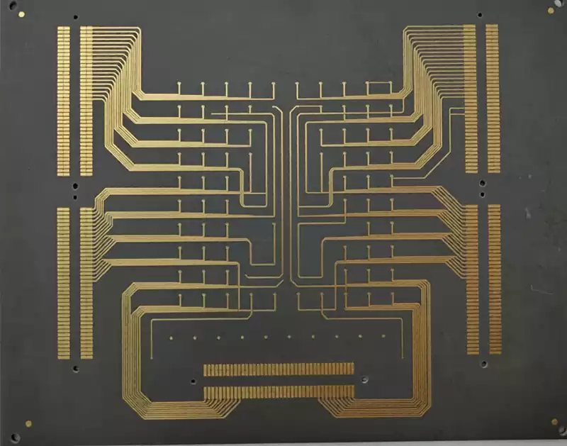
Breakthroughs in the Industrialisation Process for Glass Substrates
1.Breakthrough in Precision Laser Drilling Technology
As glass is a brittle material, the fabrication of high-density micrometre-scale through-holes is prone to cracking, chipping and breakage, presenting the primary technical challenge in the production of TGV glass substrates. The industry has achieved breakthroughs primarily through two established approaches: laser-induced etching and direct laser ablation.
In 2024, leading domestic firm Woge Optoelectronics attained mass-production-level process capabilities, consistently achieving an ultra-high aspect ratio of 150:1, with a minimum aperture precisely controlled at 3μm and a drilling efficiency of 5,000 through-holes per second. This fully meets the demands of high-end advanced packaging for high-density, high-precision hole formation in glass substrates.
2.Breakthrough in metallisation filling processes for high aspect ratio via holes
Following the formation of via holes in glass substrates, high aspect ratio micro-holes are highly prone to issues such as voids, discontinuities and uneven filling, which directly impact electrical conductivity and packaging reliability. The industry has now successfully implemented a mature composite process combining magnetron sputtering and electroplating, which reliably achieves void-free, uniform filling of through-holes with an aspect ratio of 20:1.
The adhesion, conductivity and long-term stability of the metal layer all meet mass production standards, thereby completely resolving the pain points associated with the industrialisation of glass substrate metallisation.
3.Breakthrough in High-Density Fine RDL Routing Processes
By 2025, the industry will achieve high-precision RDL re-routing processes with line widths and line spacings of ≤2μm, capable of supporting ultra-high-density interconnect requirements of 10⁴ I/O/mm². This perfectly aligns with high-end AI chips and HBM high-bandwidth packaging scenarios, addressing the final process bottleneck in high-density packaging on glass substrates.
Overall, the cost-reduction pathway for glass substrates is clear, and the advantages of scale are significant. Currently, the cost of TGV glass substrate solutions is 24% lower than that of traditional silicon TSV substrates; leveraging large-size panel-level processing technologies can further reduce production costs by 10%–30%; once the full-process mass production yield exceeds 85%, economies of scale will drive a further cost reduction of approximately 40%, meaning that in the future, the cost-performance ratio will comprehensively outperform traditional packaging substrates.
Market Potential for Glass Substrates
Based on calculations combining the global market size for advanced packaging substrates and the penetration rate of glass substrates, the industry’s growth potential is estimated as follows:
1.2026: The global market for advanced packaging substrates is projected to reach US$24.6 billion, with a glass substrate penetration rate of 5%, corresponding to a market size of US$720 million; the industry will officially enter the commercial adoption phase;
2.2027: The global advanced packaging substrate market is projected to grow to US$28.1 billion, with the penetration rate of glass substrates rising to 15%, corresponding to a market size of US$2.9 billion and a year-on-year growth rate of 305%, marking the start of a high-growth cycle;
3.2028: The global advanced packaging substrate market will exceed US$31.2 billion, with the penetration rate of glass substrates climbing to 30%, corresponding to a market size of US$7.9 billion and a year-on-year growth rate of 171%, marking the official transition into the phase of large-scale mainstream application.
Core Barriers and Competitive Landscape of Glass Substrates
1.Formulation barriers for speciality glass materials
Glass substrates designed specifically for advanced packaging differ from ordinary glass, requiring precise control of core parameters such as thermal expansion coefficient, dielectric constant, electrical insulation and flatness to meet the demands of high-frequency transmission and precision packaging. Overseas giants such as Schott and Corning have long specialised in the R&D of speciality glass, accumulating a vast number of patents, mature formulations and mass production experience, thereby establishing extremely high first-mover technical barriers.
2.Know-how Barriers in Laser Drilling Processes
Micron-level precision drilling of glass substrates imposes extremely stringent requirements on laser wavelength, power, scanning speed and process window control, necessitating long-term process fine-tuning and the accumulation of mass production experience. Different process parameters directly determine drilling yield, crack control effectiveness and through-hole consistency; new entrants find it difficult to rapidly break through established process systems, thereby creating proprietary know-how barriers.
3.Full-Process Mass Production Yield Barriers
Glass substrate packaging constitutes a precision manufacturing system involving the coordination of multiple processes, encompassing the entire workflow from substrate pre-treatment, laser via formation, cleaning, metallisation and filling, to fine-line interconnects.