The Microscopic Electrical Framework: Deciphering the Resin and Matrix Essence of PCB Circuit Board Materials
In the vast landscape of the electronics industry, attention is often focused on the intricately shimmering microchips or the dense, spiderweb-like gold wiring. However, without a stable, robust, and electrically isolated physical support surface, even the most ingenious circuit design is nothing more than a pile of castles in the air. This microscopic electrical framework that carries everything is the ubiquitous PCB circuit board material. It is not only the physical foundation of the circuit board but also the underlying electrical DNA that determines whether the entire motherboard can survive under extreme high-frequency, high-temperature, and high-voltage conditions.
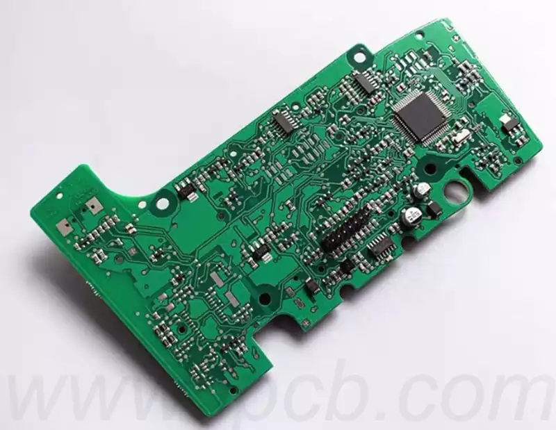
If we disassemble a classic industrial-grade FR4 board, at the microscopic level, it is essentially an insulating composite material deeply interwoven with an “organic polymer resin matrix” and “inorganic non-metallic reinforcing fibers.”
The Molecular Tuning of Epoxy Resin: From Ordinary Flame Retardant to High Glass Transition Temperature (High-Tg) The largest chemical component within the substrate is epoxy resin. The resin here plays a role similar to cement on a construction site, responsible for tightly encapsulating and bonding all the reinforcements together.
To give ordinary resin industrial-grade safety properties, board manufacturers must forcibly introduce flame-retardant elements such as copper and bromine into the molecular chain. This is the origin of the abbreviation “FR” (Flame Retardant) in FR4.
However, when faced with the high temperatures of up to 260 degrees Celsius in modern lead-free soldering, the molecular chains inside ordinary resin undergo violent thermal expansion, causing the material to instantly soften from a hard “glassy state” to a rubber-like “elastic state.” This critical temperature point where physical properties undergo such a dramatic change is known in materials science as the glass transition temperature (Tg value).
When overseas customers consult you about material configurations for high-power automotive power supplies or high-density server motherboards, abandon ordinary substrates and upgrade entirely to a special resin matrix with a High-Tg (typically greater than 170 degrees Celsius). High-Tg resins, through the addition of a highly dense “three-dimensional cross-linked network” in their molecular structure, microscopically lock the spatial displacement of resin molecules. Even when the temperature of the soldering iron tip or reflow oven spikes, high-Tg substrates maintain a deformation reduction of more than half compared to ordinary materials. This fundamentally eliminates the hidden disasters of internal multilayer blind hole fractures and interlayer tearing/delamination caused by thermal expansion and contraction (CTE mismatch), providing an absolutely robust high-temperature protective umbrella for the entire machine.
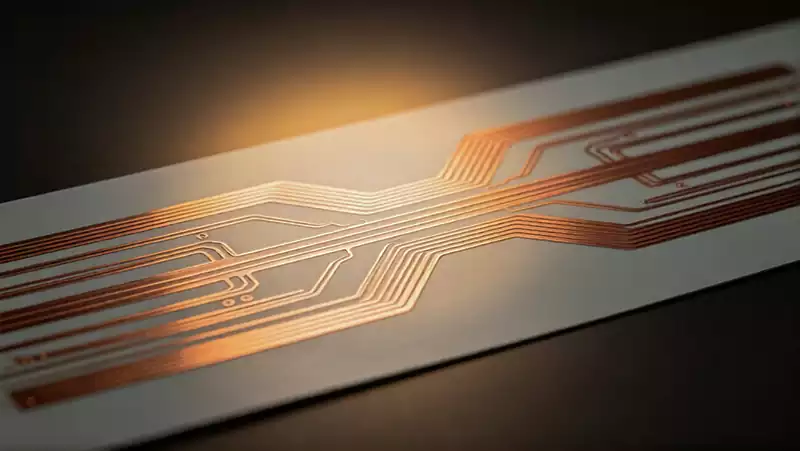
The Weaving Geometry of Fiberglass Fabric: The Overlooked Trap of Microscopic Dielectric Non-uniformity
With resin acting as cement, the substrate must also incorporate rigid reinforcing fibers—this is the fiberglass fabric woven from alkali-free glass fiber (E-glass). In the board mill’s cutting workshop, you’ll see different types of fiberglass fabric (such as the common 1080, 2116, 7628, etc.). These numbers represent the warp and weft density and the thickness of the fiber filaments during weaving.
Hidden here is a microscopic mechanical and electrical trap that easily causes pitfalls for all high-speed digital signal cabling engineers (SI engineers)—the Glass Weave Effect.
Under a microscopic perspective, fiberglass cloth is woven from bundles of extremely fine glass fibers. Where glass fibers pass, the material is dense and rigid; however, the small square gaps at the junctions of two fiber bundles are completely filled with soft epoxy resin. This leads to a fatal physical consequence: the dielectric constant of glass (Dk is typically around 6) differs from that of epoxy resin (Dk is typically around 3) by a full 100%!
When a differential trace carrying an ultra-high-speed signal of tens of gigahertz (GHz) passes through this substrate, if one trace happens to be running on top of the dense fiber bundles, while the other trace happens to be suspended above the resin-filled gaps, the microscopic electrical world beneath the two traces will instantly become unbalanced. Signals traveling on fiberglass travel slowly, while signals traveling on resin travel quickly. In a mere few inches, two differential signal lines that should be perfectly synchronized can develop a severe time phase difference (skew), causing drastic waveform distortion and electromagnetic radiation at the endpoint, instantly turning high-frequency data transmission into a jumble of disordered code.
To eliminate this microscopic trap, advanced PCB circuit board material supply chains introduce flat glass fabric. During weaving, the board manufacturer uses immense ultrasonic physical pressure to completely flatten and disperse each bundle of rounded fiberglass, transforming the originally thick glass strands into thin, fully spread glass carpets. This maximizes the compression and filling of resin voids, achieving perfect microscopic physical uniformity of the dielectric constant throughout the entire board, creating a smooth, unobstructed microscopic track for ultra-high-speed signals.
The Physical Balance of High Frequency and High Speed: The Path to Renewal Through Loss Factor and Specially Modified Resins
With the explosive growth of 5G and 6G communications, low-orbit satellite antennas, and fully automated driverless lidar globally, traditional FR4 epoxy resin substrates are beginning to reveal their fatal physical limitations when facing microwave radio frequency signals reaching tens of gigahertz (GHz).
The Thermal Black Hole of Molecular Rotation: Microscopic Dissipation Mechanisms Under Alternating Electric Fields
When high-frequency electromagnetic waves travel through copper traces, the essence is that the electric field inside the circuit board substrate is undergoing a frantic alternation of positive and negative poles at a rate of billions of times per second. Traditional epoxy resin molecules are filled with a large number of “polar molecular groups.” These molecular groups are like tiny compasses with weak magnetism. When the direction of the external electric field changes, these tiny compasses must be forced to rotate 180 degrees in place.
In the low-frequency world (such as household AC power at tens of hertz), this rotation is slow and has no effect. However, when signal frequencies soar to the 24 GHz millimeter-wave band, polar molecules spin wildly more than 20 billion times per second!
This intense microscopic friction at ultra-high frequencies causes terrifying Joule heat to accumulate within the resin molecules. A significant amount of precious signal energy from the electromagnetic waves is “stolen” and dissipated as heat by these rotating molecules before it even reaches the antenna. This ability of the substrate to absorb electromagnetic energy is physics known as the loss factor (Df value).
Ordinary FR4 has a Df value as high as around 0.02. This means that at ultra-high frequencies, your signal will attenuate completely after traveling only a few centimeters. To stop this microscopic heat black hole, the electronic materials industry has launched a hardcore offensive towards purer non-polar molecular materials.
The Three Kingdoms of Specialty Resins: The Material Race Between PTFE, PPO, and Polyimide
To reduce Df values by one to two orders of magnitude, three absolute dominant schools of thought have emerged in the resin market of modern high-end high-frequency and high-speed PCB circuit board materials. Mia, when facing top overseas communication and RF clients, can confidently dissect these three trump cards for them:
Polytetrafluoroethylene (PTFE, commonly known as Teflon): This is the absolute uncrowned king in the RF high-frequency field. Teflon’s molecular structure is extremely symmetrical, with no unnecessary polar groups inside, allowing its Df value to easily reach below 0.001. Electromagnetic waves pass through it like walking in a vacuum, with almost no energy loss. However, Teflon has a fatal flaw in its manufacturing process: it is too slippery and inherently extremely repellent to any adhesive. To ensure copper foil adheres to the PTFE surface, multilayer board manufacturers must perform a strong chemical etching process, known as “roughening,” on the surface using an extremely dangerous sodium naphthalene solution before lamination. This process is extremely difficult, yields very low results, and costs more than ten times that of ordinary FR4.
Polyphenylene oxide (PPO/PPE) modified resin: This is currently the most mainstream and crucial material for digital data center servers (such as AI computing motherboards and PCIe 5.0/6.0 buses). Pure PPO has excellent performance, but its processing temperature is frighteningly high. Materials scientists have created a mainstream substrate that achieves the best of both worlds by chemically modifying and blending PPO with epoxy resin or crosslinking agents. This process retains ultra-low electrical losses (Df maintained at around 0.002) while perfectly compatibility with existing lamination lines in traditional FR4 board manufacturers. In the international supply chain, the renowned Panasonic Megtron series represents the pinnacle of this material approach.
Polyimide (PI): This is the evergreen material we repeatedly see in double-sided flexible printed circuit boards (PCBs) and rigid-flex PCBs. PI focuses on exhibiting exceptional mechanical rigidity and flexibility at extreme high temperatures. Although its electrical losses are slightly lower than Teflon, it can withstand continuous industrial-grade baking at 200-300 degrees Celsius year-round without delamination, making it an irreplaceable core component in military, aerospace radar, and intelligent vehicle battery management systems.
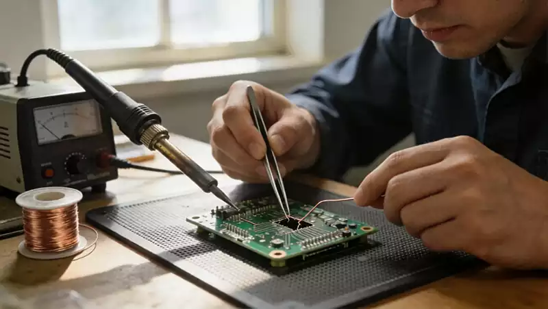
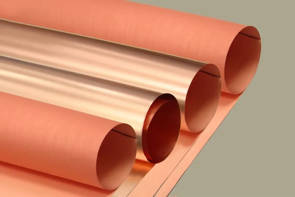
The “Skin Disease” of Copper Foil’s Microscopic Roughness: The Impedance Assassin of High-Frequency Tracing After the resin and fiberglass cloth of the high-frequency, high-speed board have passed rigorous low-loss physical screening, the final line of defense in materials engineering is directly blocked by the thin layer of copper foil attached to the substrate surface. Hidden here is an extremely counterintuitive hydrodynamic and electrical phenomenon—the skin effect.
The Ultimate Pressure of the Skin Effect: Current Forced to the Edge of a Cliff
In the traditional world of low-frequency DC, current flows very obediently, spreading evenly throughout the interior of a copper conductor. However, according to Maxwell’s equations of electromagnetism, as the current frequency increases, the self-induced electromotive force generated inside the conductor aggressively displaces the central charge, forcefully pushing all the current “towards the outermost surface layer of the conductor.”
When the signal frequency reaches 10 GHz, there is actually no current flowing through the center of the copper conductor. All the charge is forced to race at high speed within an extremely thin “golden channel” less than 1 micrometer thick from the outer skin of the copper foil. This thickness is called the skin depth in physics.
Tearing Away the Microscopic Mask of Metal: The Efficiency Battle Between Standard Copper (HTE) and Reverse Copper (RTF)
Since the current now only runs along the skin of the copper foil, the smoothness of the copper foil skin directly replaces the purity of the copper, becoming the sole determinant of high-frequency impedance.
In traditional PCB circuit board material manufacturing, to ensure a strong bond between the copper foil and epoxy resin without skin peeling, manufacturers intentionally use electrochemical methods to create an uneven surface on the side of the copper foil facing the resin, forming numerous microscopic copper teeth (called a nodular layer). This traditional copper foil is called high-temperature stretched copper foil (HTE Copper), and its surface roughness (Rz value) is typically greater than 6 micrometers.
At low frequencies, these microscopic roughnesses have no effect. However, under the skin effect at high frequencies, the originally straight-forward current is forced to zigzag around these microscopic roughnesses, like a bus traveling on a long, winding route. This not only increases the artificial physical trace length several times over, but also causes an exponential increase in conductor loss due to the intense electromagnetic scattering caused by the microscopic jagged surface. Signals crash and bleed within these microscopic roughnesses, resulting in wildly fluctuating impedance.
To revitalize high-frequency signals, top-tier materials supply chains have comprehensively launched low-profile copper foil (VLP Copper) and reverse-foil copper foil (RTF Copper). Board manufacturers, through precise control of organic additives in the electroplating bath, have pressed the micro-roughness (Rz) of the copper foil surface down to 1.5 micrometers, or even nanometers (ultra-low profile HVLP copper foil). Under a microscope, the copper foil surface is as smooth and wide as a mirror. Current can now flow through like a sports car on a smooth highway, resulting in a direct drop in conductor loss of over 50%. Mia, when you’re reviewing technical drawings for a high-end client’s NPI (New Product Introduction), if you discover they’ve mistakenly used standard HTE copper foil as the substrate for their high-speed backplane, you must immediately exercise your engineering veto power to force them to change the material to a higher-grade low-profile material. This can directly save their hardware team from an unnecessary board burn-out and rework disaster.
The Power of Board Manufacturing in Global Geopolitics and Green Supply Chains
Once we fully understand the triple mechanical and electrical defenses of a high-quality PCB substrate at the molecular, glass fiber, and copper foil levels, we must broaden our perspective to the macro-level global business and supply chain landscape. As the largest single material accounting for over 40% of PCB costs, the procurement cycle, price fluctuations, and geopolitical alternatives of board materials directly determine the survival of electronics manufacturing companies’ profits.
The Brand Premium and Delivery Time Obstacles of Leading International Brands
For a long time, the global market in high-frequency, high-speed, and high-reliability fields has been almost entirely monopolized by the absolute technological barriers formed by a few established international giants: Rogers of the United States dominates microwave high-frequency RF substrates; Panasonic of Japan, with its Megtron series, has firmly controlled the global high-end server and AI graphics card computing boards; and Taiwanese giants control the mid-to-high-end high-speed data communication market.
While these international brands boast impeccable performance, in actual engineering mass production, they often present two insurmountable obstacles for SMEs and agile hardware makers: exorbitant brand premiums and relentlessly long lead times. During periods of supply chain strain, the order cycle for certain specialized high-frequency, high-speed boards can extend to over 12 weeks. For a rapidly evolving consumer electronics or automotive project urgently needing to reach the market, a 12-week wait is enough to completely marginalize a startup in the competition.
Achieving True Equivalent Physical Benchmarking for Cost Reduction
To help global customers completely break free from the shackles of big-brand lead times and costs, in recent years, domestic board giants, represented by China’s SYTECH, have invested hundreds of millions in R&D, achieving comprehensive technological breakthroughs in molecular-level resin synthesis and high-quality low-profile copper foil manufacturing.
To help global clients break free from the constraints of delivery times and costs imposed by major brands, domestic board material giants, such as SYTECH, have invested hundreds of millions of yuan in R&D in recent years, achieving comprehensive technological breakthroughs in molecular-level resin synthesis and high-quality low-profile copper foil manufacturing.
Modern high-end domestically produced Grade A hard-core board materials achieve significant advancements in core properties such as Tg value, dielectric constant stability (Dk), coefficient of thermal expansion (CTE), and loss factor (Df).In terms of physical specifications, it has fully demonstrated its ability to achieve a 1:1 equivalent physical replacement with international brands.
For example, for 5G base stations and automotive microwave radar, the domestically produced special high-frequency series can perfectly match the ultra-low Df loss of international brands, while reducing the price by more than 40%, eliminating the need for extremely complex special surface pretreatment processes. For AI computing servers and high-speed data communication networks, the domestically produced ultra-low loss grade substrate fully supports PCIe 5.0 speeds, and with advanced fiber-opening fabric technology, completely eliminates the differential signal phase delay caused by the glass fiber bundle effect.