High frequency PCBs and high speed PCBs are often confused because both are used in advanced electronic applications. However, they are designed for different signal types and require different materials, PCB structures, and design approaches. Understanding these differences helps engineers choose the most suitable PCB for their applications.
Although these two PCB technologies share certain characteristics, including controlled impedance and low loss signal transmission, their design objectives, material properties, manufacturing requirements, and application fields differ considerably.
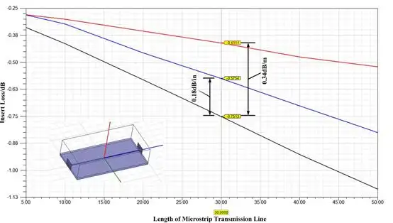
High frequency PCBs are specifically engineered for RF, microwave, and millimeter wave circuits operating at frequencies typically above 500 MHz. Their primary purpose is to minimize signal attenuation, insertion loss, impedance discontinuities, and electromagnetic interference while maintaining excellent transmission accuracy at extremely high frequencies. To achieve these objectives, high frequency laminates feature a very low dielectric constant (Dk), an exceptionally low dissipation factor (Df), low moisture absorption, and outstanding dielectric stability.
These electrical characteristics allow RF signals to propagate with minimal energy loss while maintaining consistent electrical performance under harsh environmental conditions. Consequently, high frequency PCBs are widely used in wireless communication systems, satellite communications, radar systems, RF antennas, microwave equipment, and millimeter wave sensing applications where signal accuracy and long term reliability are critical.
High speed PCBs, by comparison, are designed primarily for digital signal transmission rather than RF signal propagation. Their design emphasis is preserving signal integrity throughout high speed data transmission by minimizing propagation delay, timing skew, crosstalk, signal reflection, and waveform distortion. Instead of focusing solely on operating frequency, high speed PCB design concentrates on maintaining clean digital waveforms at increasingly higher data rates.
These boards typically employ low loss, high Tg FR 4 or other advanced laminate materials that offer stable dielectric properties, excellent dimensional stability, and low thermal expansion. Such characteristics make high speed PCBs ideal for servers, computer motherboards, networking equipment, storage systems, industrial controllers, and other electronic products requiring reliable high bandwidth digital communication.
The differences between high frequency and high speed PCBs become even more apparent when examining their engineering requirements. High frequency PCBs are intended for RF analog signals operating in microwave and millimeter wave frequency bands, where minimizing conductor loss and dielectric loss is the primary design objective. High speed PCBs, however, are designed for high speed digital interfaces that may operate across a broad frequency spectrum ranging from several tens of megahertz to multiple gigahertz, with the principal objective being reliable data transmission rather than maximizing operating frequency.
Their physical construction also differs substantially.High frequency PCB layouts generally require ultra fine trace widths, narrow trace spacing, and thinner dielectric layers to reduce insertion loss and suppress electromagnetic interference.High speed PCB layouts place greater emphasis on impedance control, differential pair routing, and trace length matching to ensure synchronized signal arrival while maintaining manufacturing yield. Consequently, trace widths and board thicknesses can often be optimized according to impedance requirements rather than being minimized.
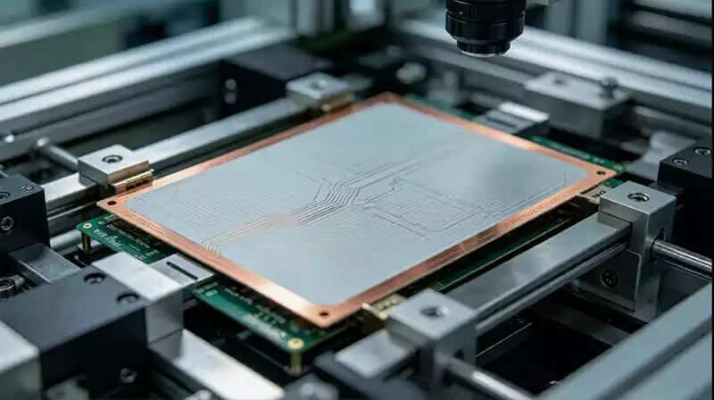
Material selection represents another major distinction. High frequency PCBs typically utilize PTFE based laminates or other advanced RF materials such as Rogers®, Taconic®, or similar low loss substrates. These materials provide extremely low dielectric constants and dissipation factors, significantly reducing signal attenuation at microwave frequencies. High speed PCBs generally employ high Tg FR 4, low loss epoxy laminates, or advanced glass reinforced composite materials that provide an excellent balance between electrical performance, manufacturability, and cost while meeting the signal integrity requirements of modern digital systems.
Manufacturing requirements also vary considerably between the two technologies. High frequency PCB fabrication demands exceptionally tight process control, including precise dielectric thickness, highly uniform copper plating, extremely smooth conductor surfaces, and stringent impedance control to minimize conductor loss and RF discontinuities. These requirements necessitate specialized fabrication equipment and advanced manufacturing expertise. In contrast, high speed PCBs can usually be manufactured using conventional precision PCB fabrication processes, provided that impedance control, dimensional accuracy, and differential routing requirements are carefully maintained, resulting in lower manufacturing costs and higher production efficiency.
PCB layout priorities further distinguish these technologies. High frequency PCB design focuses primarily on RF electrical performance by optimizing impedance matching, conductor surface roughness, dielectric properties, copper adhesion, and transmission line characteristics to minimize RF losses. High speed PCB design, on the other hand, concentrates on maintaining signal integrity through careful management of differential pair routing, propagation delay, trace length matching, timing synchronization, and crosstalk reduction to ensure reliable high speed digital communication.
These differences naturally lead to different application areas. High frequency PCBs are extensively used in wireless communication infrastructure, satellite communication equipment, microwave and millimeter wave radar systems, RF front end modules, antennas, aerospace electronics, and advanced sensing technologies, where extremely low signal loss and excellent electromagnetic performance are essential. High speed PCBs are widely employed in computer motherboards, servers, high speed storage devices, industrial automation equipment, precision instrumentation, networking hardware, and telecommunications systems that require stable, high bandwidth digital data transmission.
Although both high frequency and high speed PCBs are designed to support advanced electronic systems, they solve fundamentally different engineering challenges. High frequency PCBs deliver outstanding performance for RF and microwave analog circuits through ultra low dielectric loss and superior electromagnetic stability, whereas high speed PCBs are optimized for preserving digital signal integrity through controlled impedance, low propagation delay, and effective suppression of crosstalk and signal reflections.