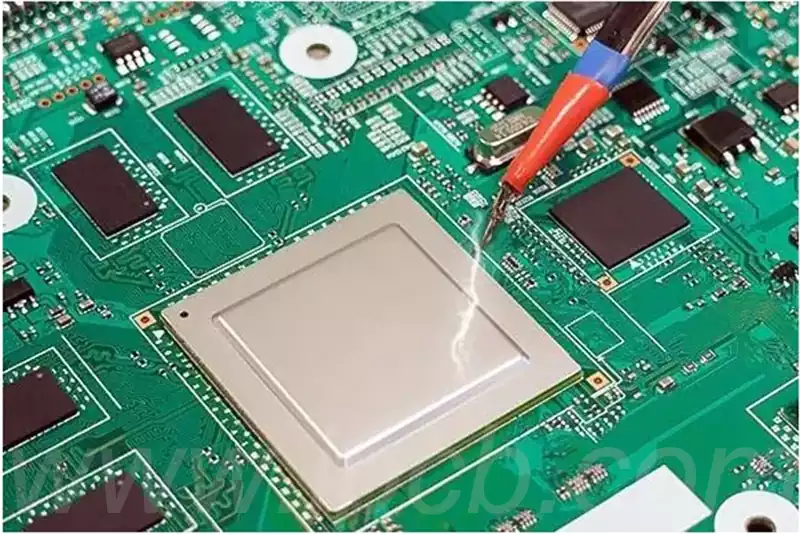
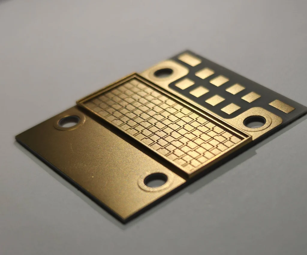
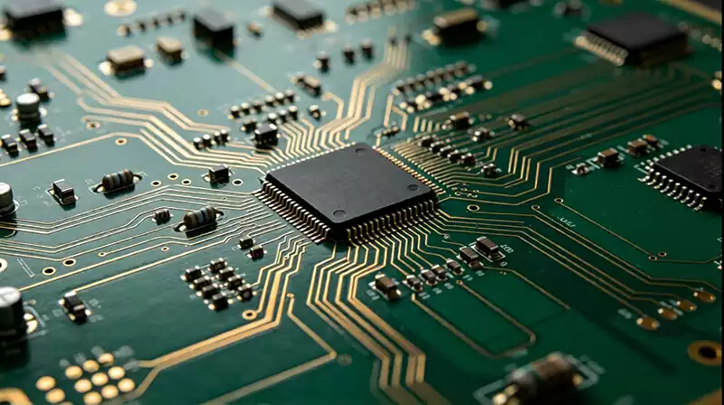
PCB wiring is the process of creating copper traces on a printed circuit board to establish electrical interconnections between components, power supplies, and ground structures. In the PCB design workflow, routing converts the logical connectivity defined in the schematic into physical conductive paths on the circuit board. This design stage not only determines the electrical connectivity and functional integrity of the entire board but also directly affects signal transmission quality, power distribution efficiency, and the overall performance of the finished PCB under actual operating conditions.
For simple, low-speed circuits, PCB routing may appear to involve little more than establishing basic electrical connections between components. However, modern high-density and high-performance PCBs are subject to much stricter design and manufacturing requirements. Parameters such as trace width, clearance, trace length, routing layer selection, characteristic impedance, via placement, signal return paths, and coupling between adjacent traces can all have a significant impact on electrical performance. Improper routing can lead to signal crosstalk, reflections, excessive voltage drop, electromagnetic interference (EMI), and inadequate thermal performance. A well-planned routing strategy helps ensure that the finished PCB meets both electrical performance requirements and manufacturing requirements for volume production.
High-quality PCB routing begins before the actual traces are drawn. Designers need to consider component placement, layer stackup, power distribution, critical signal paths, and overall design constraints as an integrated system. Treating each design element independently can significantly increase routing complexity and create conflicts or manufacturing issues later in the design process.
Routing should prioritize critical signal paths. High-speed clock signals, differential pairs, sensitive analog signals, primary power paths, and signal nets that are sensitive to timing or noise all require dedicated routing rules. Cadence design guidelines emphasize coordinating component placement and routing strategies around critical signals. Altium design guidelines also recommend defining key constraints such as trace width, clearance, impedance, trace length, and topology before detailed routing begins.
The PCB layer stackup has a decisive impact on routing quality. In multilayer PCBs, signal layers should be properly arranged with power and ground planes, while vias provide electrical connections between routing layers. A properly engineered stackup enables controlled impedance and provides stable, predictable return-current paths for high-speed signals. An inappropriate layer arrangement can significantly increase routing complexity and make it difficult to meet the requirements of high-speed circuits.
Key PCB Routing Parameters and Their Impact on Electrical Performance
1.Trace Width Design Requirements
Trace width is one of the most fundamental and important parameters in PCB routing. There is no universal trace width suitable for every circuit. Compared with low-current signal traces, power traces generally require a larger copper cross-sectional area. A smaller effective conductor cross-sectional area results in higher DC resistance and greater Joule heating during operation, which can affect power delivery stability and reduce PCB service life.
For high-speed signals requiring controlled impedance, trace width is an essential part of the transmission-line structure. The resulting characteristic impedance is determined by factors including trace geometry, copper thickness, dielectric thickness, dielectric material properties, and the distance between the trace and its reference plane. Altium design guidelines recommend developing routing rules according to the specific electrical requirements of different interfaces rather than applying a single trace-width rule to all signal nets.
This principle is particularly important for high-speed PCBs. An abrupt change in the width of a controlled-impedance trace can create an impedance discontinuity and directly degrade signal integrity. Designers should therefore calculate the target trace width based on the actual PCB stackup and electrical requirements, then verify the result against the PCB manufacturer’s process capabilities to ensure that the design is manufacturable and suitable for volume production.
2.Trace Clearance Requirements
The clearance between adjacent traces affects both PCB manufacturing yield and electrical isolation. Excessively small spacing increases electromagnetic coupling between traces and can cause signal crosstalk. The faster the signal edge rate and the longer the parallel routing distance, the more significant the crosstalk can become.
Trace clearance must be determined according to both PCB fabrication capabilities and the electrical characteristics of the signals. Differential pairs, clock signals, precision analog signals, and high-frequency switching power nodes may require different clearance requirements. Designers cannot apply a single spacing rule to every circuit. Instead, clearance should be determined by considering the layer stackup, routing geometry, signal characteristics, manufacturing capabilities, voltage requirements, and applicable design rules.
For high-speed interfaces with limited routing space, signal-integrity simulation and electromagnetic field analysis can be used to optimize trace spacing more precisely.
Key Considerations for High-Speed PCB Routing
As signal edge rates continue to increase, a PCB trace can no longer be treated simply as a conductive wire. It behaves as a transmission-line structure with distributed electrical characteristics. Under these conditions, the electrical length of the trace becomes a critical design parameter, and the routing strategy directly affects signal reflections, insertion loss, timing accuracy, and overall signal integrity.
In high-speed circuits, PCB traces are not merely interconnects between components. They are an integral part of the electrical system.
High-speed PCB routing must strictly follow controlled-impedance requirements while maintaining the integrity of the signal reference plane. Critical signal paths should maintain consistent geometry and avoid unnecessary layer transitions to minimize impedance discontinuities.
Differential-pair routing requires even tighter control. The two traces in a differential pair should maintain a consistent spacing and stable electromagnetic coupling along the entire route. Trace length, via structures, reference planes, and geometric characteristics should remain highly symmetrical. Modern high-speed design practices also emphasize maintaining a continuous reference structure, minimizing unnecessary serpentine routing, and avoiding excessive bends that may introduce signal-integrity issues.
Return Path and Trace Length Optimization
The return path is one of the most easily overlooked aspects of PCB routing. Signal transmission does not occur only through the signal trace. The corresponding return current travels through the PCB structure to complete the current loop.
In high-speed PCBs, a continuous reference plane directly beneath the signal trace provides a stable and predictable return-current path. If a high-speed trace crosses a split, void, or cutout in its reference plane, the return current must divert around the discontinuity. This increases the current-loop area and can result in greater electromagnetic interference and signal-integrity problems. Therefore, critical high-speed signals should be routed over a continuous reference plane, and crossing plane splits should be avoided.
Layer transitions also require careful consideration of the return-current path. When a signal changes layers through a via, the return current needs an appropriate transition path as well. Ignoring the return path can result in hidden impedance discontinuities even when the signal connection itself is electrically correct.
Where electrical requirements permit, PCB routing should generally follow the principle of keeping traces short and direct. Excessively long traces increase parasitic resistance, capacitance, and inductance. As signal speed increases, these parasitic effects can cause greater propagation delay, ringing, and other signal-integrity problems.
However, short and direct routing is not appropriate for every application. Some high-speed interfaces and memory buses require strict length matching and defined topologies. In such cases, intentionally extending trace length may be necessary. The overall objective is to eliminate unnecessary routing while satisfying the electrical requirements of the interface.
Detailed Design of Trace Geometry and Vias
Trace geometry directly affects high-speed signal transmission stability. Both traditional PCB design practices and modern high-speed design guidelines generally discourage the use of 90-degree corners for high-speed traces. Abrupt changes in trace geometry can create impedance discontinuities and adversely affect signal transmission.
45-degree bends or smooth curved corners provide a more gradual transition and can help reduce signal-integrity issues. For ordinary low-speed circuits, trace corners generally have little effect on electrical performance. High-speed and RF circuits, however, are much more sensitive to trace geometry because the physical structure of the transmission line itself forms part of the electrical design.
For critical differential pairs and RF signals, curved routing can be used where appropriate to minimize unnecessary changes in trace geometry.
Vias are essential structures in multilayer PCB routing because they provide electrical connections between different layers. However, a via is not an ideal lossless interconnect. It introduces parasitic inductance and capacitance and can create impedance discontinuities in high-speed and high-frequency transmission paths.
Excessive layer transitions can increase signal loss and create signal-integrity problems, with the impact becoming more significant at higher frequencies. Conventional low-speed control signals are generally less sensitive to via characteristics. High-speed interfaces and RF circuits, however, require strict control of via count and geometry. Designers should minimize via stubs, optimize via structures, and provide appropriate return-current paths. Critical high-speed signal paths should use as few layer-transition vias as practical.
Routing Strategies for Power and Mixed-Signal Circuits
Power routing follows a different design philosophy from signal routing. Its primary concerns include current-carrying capacity, voltage drop, temperature rise, loop area, and power integrity.
An undersized power trace increases DC resistance and can result in excessive heating and unacceptable voltage drop. High-current power paths may require wider traces, heavier copper, large copper pours, or dedicated power planes. The appropriate parameters should be determined based on operating current, allowable temperature rise, copper thickness, operating environment, and PCB fabrication capabilities.
The quality of power and ground routing directly affects signal integrity. A poorly designed power distribution network (PDN) can introduce voltage fluctuations and electrical noise that interfere with sensitive circuits. In mixed-signal PCBs, power distribution, grounding, and signal return paths should therefore be planned together rather than treating the power network as an afterthought after signal routing is complete.
The primary challenge in mixed-signal PCB routing is controlling interference between digital and analog circuitry. Fast voltage transitions in high-speed digital signals can generate electrical noise through common impedance, capacitive coupling, inductive coupling, and discontinuous return-current paths.
Sensitive analog traces should be routed over an appropriate continuous reference plane and kept away from high-frequency switching nodes. High-current switching paths should not run in parallel over long distances with low-level sensor or precision analog signals.
Mixed-signal PCB design does not necessarily require rigid physical partitioning of the entire board into separate digital and analog regions. Instead, the layout, power distribution, grounding structure, and return-current paths should be optimized according to the overall circuit architecture. A well-engineered power and ground plane structure is often more effective at controlling interference than simply separating components into different physical areas.
Design for Manufacturability and Common PCB Routing Issues
PCB routing must satisfy both electrical-performance requirements and manufacturing constraints. A design that passes electrical connectivity checks in PCB design software may still be difficult or impossible to manufacture if it exceeds the fabricator’s process capabilities.
Parameters such as trace width, clearance, via hole diameter, annular ring, copper thickness, aspect ratio, and layer-to-layer registration accuracy must remain within the manufacturer’s specified process window.
Before detailed routing begins, designers should establish comprehensive design rules and use Design Rule Checking (DRC) to identify potential issues such as insufficient clearance, abnormal trace widths, and open circuits at an early stage. This helps improve manufacturing yield and reduces costly design iterations.
Manufacturing tolerances can directly affect impedance accuracy in high-end high-speed PCBs. The performance of a controlled-impedance transmission line depends on dielectric thickness, copper thickness, trace width, and material properties. Variations in these manufacturing parameters can cause the finished impedance to deviate from the target value and affect overall circuit performance.
Many PCB routing problems originate from an overly standardized routing approach. Low-speed control traces, high-current power traces, RF transmission lines, and high-speed differential pairs have very different electrical and manufacturing requirements. Applying the same routing rules to all of them can lead to excessive crosstalk, increased insertion loss, timing skew, discontinuous return paths, and excessive heating.
A reverse workflow in which designers route first and verify electrical parameters later can also result in extensive redesign. Establishing differentiated routing constraints before routing begins is therefore one of the most effective ways to prevent these issues.
Standardized PCB Routing Design Process
A reliable PCB routing process should follow a clear priority structure.
During the initial design stage, component placement should be based on signal flow. Critical signal nets should be identified and classified in advance, while the optimal PCB layer stackup should be determined according to the electrical requirements of the circuit.
Once component placement and the layer stackup have been established, designers should prioritize power paths and critical signal paths. High-speed differential pairs should be routed according to controlled-impedance and length-matching requirements. Sensitive analog signals should be routed with appropriate isolation and noise-control measures. Ordinary low-speed signals can then be routed around the critical signal paths.
After routing is completed, the design should undergo comprehensive Design Rule Checking (DRC). Depending on the application, designers should also perform signal-integrity (SI), power-integrity (PI), thermal, and electromagnetic-compatibility (EMC) analysis.
High-speed interfaces should not be verified solely through visual inspection. Impedance calculations and simulation are required to validate the electrical performance of critical transmission paths. As data rates continue to increase, PCB traces are increasingly treated as essential parts of the electrical transmission system, making simulation and manufacturing-process verification more important than ever.
PCB routing is far more than simply drawing conductive paths. Copper traces are an integral part of the electrical system, and their geometry, length, spacing, layer position, and coupling to reference planes directly influence the performance of the finished PCB.
For conventional PCBs, the primary routing objectives are reliable electrical connectivity and manufacturing compliance. For high-speed, RF, and high-current precision circuits, PCB wiring is a system-level engineering discipline involving impedance control, signal optimization, return-path management, crosstalk suppression, thermal design, and manufacturing-tolerance control.