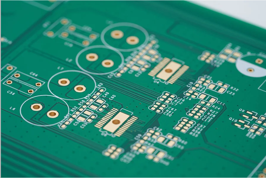
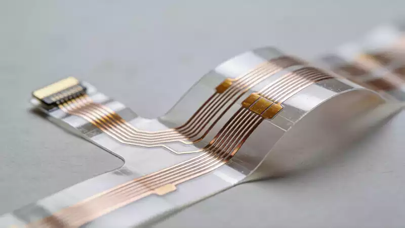
RF electronics design requires much more than connecting components according to a schematic. When a circuit operates at radio frequencies, the physical structure of the PCB becomes part of the electrical system. Trace geometry, dielectric thickness, copper thickness, grounding, component placement, vias, connectors, and even the distance between adjacent circuits can affect how an RF signal travels across the board.
At lower frequencies, a PCB trace can often be treated mainly as an electrical connection between two components. As frequency increases, that assumption becomes less reliable. The trace behaves more like a transmission line, and its surrounding electromagnetic environment starts to have a direct influence on signal integrity. A small change in trace width or dielectric thickness can affect impedance, while an interruption in the reference plane can change the return-current path. These effects are why RF electronics design needs to consider the electrical circuit and physical PCB structure together.
For engineers working on wireless communication equipment, RF modules, antennas, filters, amplifiers, transceivers, sensors, and other high-frequency electronics, the PCB should therefore be considered during the early stages of the design rather than after the schematic has already been completed.
The PCB Becomes Part of the RF Circuit
One of the most important differences between conventional PCB design and RF electronics design is the role of the interconnection itself. An RF signal does not simply travel from one component pin to another through a piece of copper. The signal exists within an electromagnetic field that is influenced by the conductor, its reference plane, the dielectric material between them, and nearby conductive structures.
This is particularly important when designing controlled-impedance transmission lines. A commonly used RF interface has a characteristic impedance of 50 ohms, but achieving that impedance is not simply a matter of selecting a particular trace width. The required geometry depends on the PCB stackup, dielectric thickness, copper thickness, material properties, and the transmission-line structure being used. Microstrip, stripline, and grounded coplanar waveguide structures can all be used in appropriate RF applications, but their physical configurations and electromagnetic behavior are different.
For this reason, impedance control should be considered when the PCB stackup is being developed. If the dielectric thickness changes after the routing has been completed, the original trace dimensions may no longer provide the intended impedance. The same problem can occur when the finished copper thickness differs from the value assumed during the design process.
A practical RF design therefore starts by defining the electrical requirements and then translating those requirements into a physical PCB structure. The target impedance, operating frequency, material construction, layer arrangement, copper thickness, and manufacturing tolerances all need to be considered together.
Stackup, Grounding and Routing Need to Work Together
The PCB stackup has a direct influence on RF performance because it establishes the relationship between signal conductors and their reference planes. A signal layer positioned close to a continuous ground plane can provide a more predictable transmission-line structure and help keep the return current close to the signal path. Analog Devices, for example, describes the use of a continuous ground plane beneath RF routing as an important part of maintaining controlled impedance and short return paths.
Grounding is therefore not simply a matter of providing enough copper area. The location and continuity of the reference plane matter as well. When an RF trace crosses a gap or interruption in its reference plane, the return current may need to find another path. That change can increase the effective loop area and alter the electromagnetic behavior of the interconnect. For high-frequency circuits, this can contribute to unwanted coupling and radiation.
The same principle applies when an RF trace changes layers. A via changes the physical geometry of the transmission line, and at sufficiently high frequencies, via structures can introduce significant discontinuities. Unnecessary layer transitions and long via stubs should therefore be avoided where the application is sensitive to these effects.
RF routing also needs to take the entire signal path into account. A connection between an RF integrated circuit and an antenna, connector, filter, or matching network should be considered as one continuous transmission structure rather than as a series of independent PCB traces. Sudden changes in width, poorly controlled transitions, excessive bends, or inappropriate clearances can affect the behavior of that path.
Ground vias can also be used around RF structures to improve the connection between ground regions and help control unwanted coupling. However, the appropriate arrangement depends on the operating frequency and the particular PCB structure. There is no universal via spacing or routing dimension that can be applied to every RF board. The physical dimensions should be determined from the intended electrical performance and actual stackup.
Component Placement and Isolation Are Equally Important
RF performance can be affected before a single trace is routed because component placement determines how much interaction exists between different sections of the circuit. A board may contain an RF receiver, transmitter, power supply, processor, memory, clock circuits, and other interfaces at the same time. If these functional blocks are placed without considering their signal relationships, the routing stage can become much more difficult.
Sensitive RF inputs generally benefit from a carefully controlled physical environment. High-power RF outputs, fast digital interfaces, switching power circuits, and clock signals can introduce unwanted energy into nearby sensitive areas. Keeping functional blocks appropriately arranged can reduce the amount of unnecessary coupling and make the intended signal paths easier to maintain.
This does not mean that every RF and digital section must be placed on completely isolated ground islands. In many mixed-signal designs, an uninterrupted ground plane can provide a better-defined return path than artificially dividing the plane. The appropriate grounding architecture depends on the circuit, current paths, layer structure, and system requirements. Recent PCB design guidance also emphasizes making grounding and placement decisions early because these decisions influence routing and the final layer stackup.
Power distribution deserves similar attention. RF circuits can be sensitive to noise on their supply rails, particularly when the power system contains switching circuits or other rapidly changing loads. Power routing, bypassing, component placement, and grounding should therefore be considered together with the RF signal path rather than treated as a separate task.
Material selection is another part of the same process. At higher frequencies, dielectric properties and material losses become increasingly relevant to signal behavior. The appropriate PCB material depends on the operating frequency, electrical loss requirements, mechanical construction, thermal requirements, and manufacturing process. The material should not be selected independently from the stackup because the final transmission-line geometry depends on the actual dielectric structure.

From RF Design to Manufacturing and Verification
A technically sound RF electronics design still needs to be translated accurately into a manufactured PCB. This is where manufacturing tolerances become important. Variations in trace width, dielectric thickness, copper thickness, layer registration, drilling, and material construction can influence the final electrical characteristics of an impedance-controlled RF structure.
For example, a particular RF device may specify a 50-ohm coplanar waveguide with dimensions based on a specific PCB stackup. Those dimensions cannot simply be copied to another board and expected to produce the same result if the dielectric thickness, copper thickness, or material construction has changed. An actual Analog Devices RF device datasheet illustrates this point by specifying its recommended RF transmission-line dimensions together with the associated dielectric thickness and copper construction, and notes that alternate stackups require different recommendations.
This is why RF PCB manufacturing should be considered during design review. The intended impedance, layer construction, material, copper thickness, and relevant tolerances need to be communicated clearly before fabrication. When the design depends on tight electrical characteristics, the manufacturing process should be capable of maintaining the physical dimensions required by the RF design.
Verification is also more involved than simply checking whether the PCB passes basic design-rule checks. Depending on the application, engineers may use simulation and laboratory measurements to evaluate impedance, insertion loss, return loss, isolation, and other RF characteristics. Measurement results can then be compared with the expected behavior to determine whether the physical board is performing as intended.
This creates a continuous relationship between design and manufacturing. The schematic defines the circuit, the stackup establishes the physical environment, the layout determines the signal paths, manufacturing creates the physical structure, and testing confirms how that structure behaves in practice.
Good RF electronics design is ultimately about controlling the relationship between an RF signal and the physical environment through which it travels. The schematic is only one part of that process. Once the signal reaches the PCB, the transmission line, reference plane, dielectric material, vias, component placement, grounding structure, and manufacturing tolerances all become part of the RF system.
For this reason, RF PCB design should begin with the stackup and signal architecture rather than treating PCB layout as the final step after circuit design. Controlled impedance needs to be considered alongside material selection and dielectric thickness. Grounding needs to provide a predictable return path. Component placement needs to account for sensitive and noisy circuit sections. Routing needs to preserve the intended transmission-line structure, while manufacturing needs to reproduce the physical dimensions assumed during design.
When these factors are considered together, the transition from RF circuit design to PCB fabrication becomes much more predictable. That integrated approach is particularly important for high-frequency electronics where a small physical change can produce a measurable electrical difference.