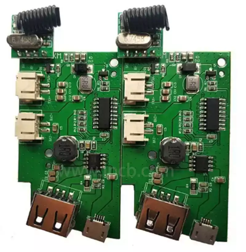
A button circuit board converts a physical press into an electrical command. It may control a household appliance, industrial panel, medical device, automotive interface or handheld product. Although the circuit appears simple, an unreliable button can produce missed commands, repeated inputs or intermittent operation that is difficult to reproduce during inspection.
The problem is rarely caused by one factor alone. Reliable operation depends on the switch mechanism, contact surface, PCB layout, soldering process, firmware filtering and mechanical enclosure working together. Understanding this complete signal path is the most effective way to prevent unstable input behavior.
How a Button Press Becomes an Electrical Signal
Most button inputs use a normally open contact. Pressing the button connects two conductive points, allowing the controller to detect a change in voltage. A pull-up or pull-down resistor maintains a defined logic state when the button is not pressed.
Depending on the product, a button circuit board may use tactile switches, metal domes, carbon contacts, conductive rubber keypads or membrane switches. Each technology creates the same basic input function but has different requirements for contact force, surface finish, alignment and environmental protection.
A tactile switch contains its own metal contact mechanism and is soldered directly to the PCB. Metal domes and conductive rubber keys instead make contact with exposed PCB pads. These exposed contact areas become part of the switching mechanism, so their geometry and surface condition directly affect performance.
Contact Resistance Creates Intermittent Inputs
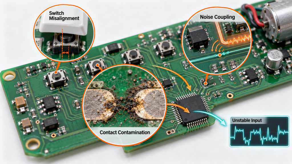
A button does not always change instantly from a perfectly open circuit to a perfectly closed circuit. Oxidation, contamination, wear and insufficient contact pressure can increase resistance at the switching point.
When contact resistance becomes unstable, the controller may detect a press only when the user applies additional force. In severe cases, the button works during initial testing but becomes intermittent after exposure to humidity, dust or repeated operation.
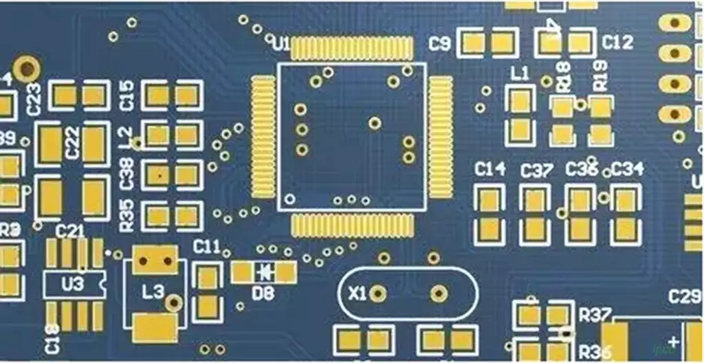
The contact pads on a button circuit board must therefore remain clean and flat. For exposed keypad contacts, the selected surface finish should provide consistent conductivity without creating an uneven surface. Gold-based finishes are often used where low contact resistance and corrosion resistance are important, while the specific finish should still match the product environment and expected operating life.
Flux residue must also be controlled. Residue near high-impedance input circuits can retain moisture or create leakage paths between adjacent conductors. This may generate false inputs even though the mechanical button has not been pressed.
Switch Bounce Can Produce Several Commands From One Press
Mechanical contacts do not close once and remain stable immediately. They can make and break contact several times over a short interval before settling. This behavior is known as switch bounce.
Without suitable filtering, one press may be interpreted as several commands. A volume button might jump multiple levels, or a menu key might move past the intended selection. The defect may look like a damaged switch even when the component is operating normally.
Debouncing can be implemented in hardware, firmware or both. Hardware solutions commonly use resistors, capacitors or dedicated input-conditioning devices. Firmware solutions verify that the input remains stable for a defined interval before accepting the change.
For a button circuit board, the appropriate debounce method depends on the switch characteristics, response-time requirements and electrical noise surrounding the input. Excessively short filtering allows repeated triggers, while excessive filtering makes the interface feel slow.
PCB Layout Affects Input Stability
Button signals usually operate at low current, making them vulnerable to coupling from motors, relays, switching regulators and high-current traces. Long button traces routed beside noisy conductors can collect interference and cause false activation.
The layout of a button circuit board should keep input paths reasonably short and provide a clear return path. Sensitive inputs should be separated from switching nodes, motor outputs and rapidly changing power traces. Where the product uses external buttons connected through cables, filtering and electrostatic-discharge protection may also be necessary near the connector.
Moisture creates an additional risk when exposed contact patterns are used. Closely spaced pads may develop leakage paths after contamination or condensation. Solder-mask clearance, contact spacing and enclosure sealing should therefore be considered together rather than evaluated as unrelated details.
Assembly Quality Changes the Mechanical Response
The height and alignment of a tactile switch determine how it interacts with the external keycap. A switch mounted at an angle may still pass electrical inspection, but the enclosure can apply force unevenly or prevent the actuator from travelling far enough.
Uneven solder paste, component movement during reflow and incorrect switch orientation can all affect the finished interface. Because the user interacts mechanically with the assembled product, electrical continuity alone cannot confirm acceptable operation.
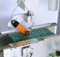
Inspection of a button circuit board should verify switch position, solder-joint formation and component height. For dense assemblies, automated optical inspection can identify offset switches and insufficient solder, but a mechanical press test is still needed to evaluate the interaction between the PCB and enclosure.
The Enclosure Can Create a PCB Failure
Some apparent PCB failures originate in the product housing. A keycap may be too short, a rubber keypad may be compressed unevenly or a plastic guide may push the switch sideways. Dimensional variation in molded parts can also change the actuation force between production batches.
For this reason, the button circuit board should be tested both independently and after installation. Board-level testing verifies the electrical input, while unit-level testing confirms key travel, force and alignment.
This distinction is especially important for conductive rubber keypads. The rubber structure controls both the return force and the contact pressure. If the keypad is misaligned, even perfectly manufactured PCB contacts may produce missed presses.
Manufacturing Tests Must Reproduce Real Operation
A simple continuity check confirms that a circuit can close, but it does not show whether every press produces one clean command. Functional testing should monitor the controller response while the switch is physically operated.
Testing a button circuit board under realistic conditions can reveal several different failure modes. A light press exposes marginal actuation, repeated presses reveal bounce or weak solder joints, and operation near motors or relays identifies noise sensitivity. Environmental testing may also be needed when the product will encounter moisture, cleaning chemicals or large temperature changes.
For projects entering production, iPCB can combine component verification, solder-paste inspection, AOI and functional button testing within the same PCBA manufacturing process. Test requirements should specify the expected command response rather than only requiring electrical continuity.
Reliable Buttons Depend on the Complete Assembly
Stable input operation requires more than selecting a durable switch. Contact materials, debounce behavior, PCB routing, soldering accuracy and enclosure dimensions must all support the same mechanical and electrical function.
When these factors are evaluated together, a button circuit board can deliver consistent response throughout production and long-term use. This system-level approach prevents missed presses and repeated commands more effectively than replacing switches after the product has already failed.