A circuit board texture reflects the combination of materials, conductive patterns, protective coatings, and surface finishes that give a printed circuit board its recognizable appearance. Fine copper traces, metallic pads, solder mask, vias, and printed markings each contribute different visual details. Understanding these features helps engineers distinguish the physical structure of a PCB from decorative patterns used in digital graphics, product presentations, and technical illustrations.
What Defines Circuit Board Texture
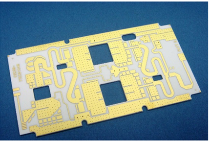
A printed circuit board consists of several materials and patterned layers. The substrate provides mechanical support and electrical insulation, while copper layers form the conductive traces, pads, and planes that connect electronic components. On the outer surface, solder mask typically covers most of the copper while leaving designated connection points exposed.
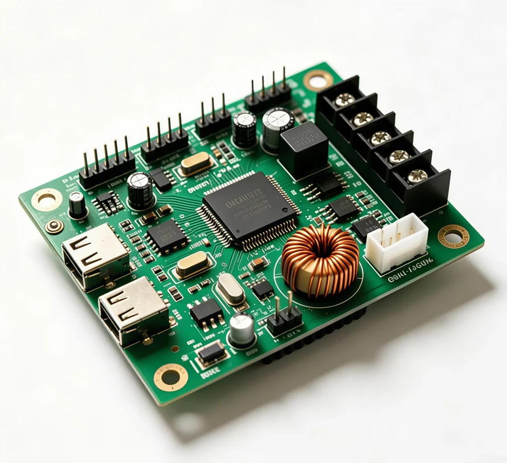
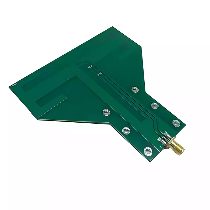
The familiar green appearance of many boards comes from the solder mask, although manufacturers can use other colors and surface appearances. A glossy coating reflects light more directly, while a matte coating diffuses reflections and produces a softer visual effect. The underlying copper layout adds fine lines, angular paths, circular pads, and geometric patterns that make a circuit board texture recognizable even when most of the conductive metal is covered.
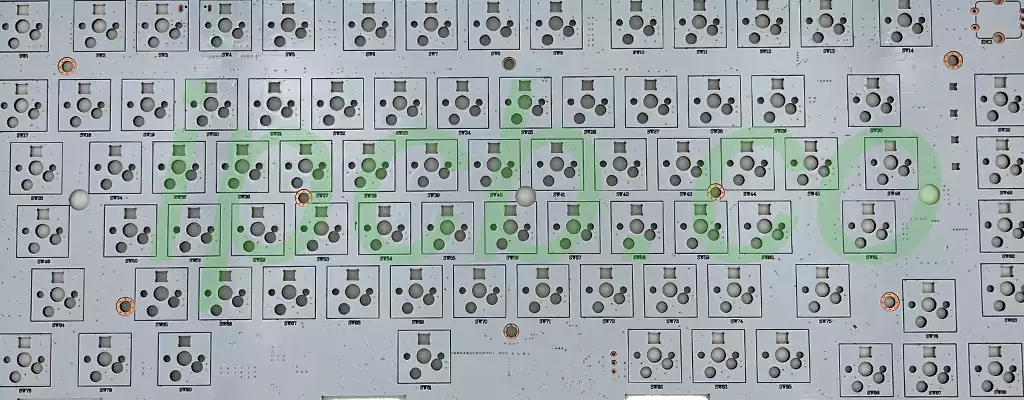
Other visible details come from silkscreen markings and exposed metallic areas. Component reference numbers, polarity symbols, logos, and assembly instructions are commonly printed on the surface. Exposed pads may appear silver, gold-colored, or metallic depending on the selected surface finish. Vias and plated holes introduce additional circular features that connect conductive layers or provide electrical and mechanical interfaces.
These elements should be distinguished from the substrate itself. The board’s surface appearance mainly reflects its coating and copper layout, whereas the laminate’s material characteristics may be more apparent at cut edges, drilled holes, or exposed cross-sections.
How Solder Mask and Surface Finish Affect Circuit Board Appearance
Solder mask is one of the most visible factors influencing PCB appearance. Its color, reflectivity, coverage, and surface consistency determine how the underlying copper pattern is perceived. Green is widely used, but black, blue, red, white, and other colors are also available. The best choice depends on manufacturing requirements and the intended visual presentation rather than color alone.
A circuit board texture can look noticeably different under different lighting conditions. Direct illumination may create bright reflections on exposed metal, while diffuse lighting reveals the overall pattern with fewer harsh highlights. Macro photography can make small surface features more prominent, but excessive sharpening or contrast adjustment may exaggerate normal variations and make a manufactured board appear defective.
Surface finish also changes the appearance of exposed copper pads. Common finishes include hot air solder leveling (HASL), electroless nickel immersion gold (ENIG), and organic solderability preservative (OSP). These options have different material characteristics, solderability requirements, and storage considerations. Their visual differences are useful for identifying surface features, but appearance alone does not establish whether a finish meets the required electrical or manufacturing specifications.
Solder mask quality and surface finish should therefore be evaluated separately. A consistent coating does not necessarily indicate that the exposed pads have the correct finish, and a metallic-looking pad does not prove that its electrical or soldering performance is acceptable. Technical assessment requires the relevant fabrication specifications and inspection criteria.
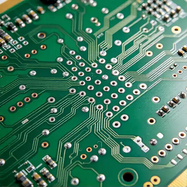
What PCB Circuit Board Surface Details Can Reveal
Visual inspection can help identify potential manufacturing concerns. Uneven solder mask coverage, unwanted exposed copper, damaged coating, contamination, or inconsistent pad appearance may indicate that further examination is needed. The significance of these observations depends on their location, severity, and the requirements of the finished board.
For example, exposed copper in an area that should be covered by solder mask may indicate a registration or fabrication issue. Discoloration around a pad could have several causes, including the surface finish, contamination, or storage conditions. A photograph alone may not provide enough information to identify the cause confidently.
The same principle applies when evaluating a circuit board texture for technical documentation. Reflections can make a smooth coating appear uneven, and shadows may exaggerate the apparent depth of traces or holes. Consistent lighting, appropriate magnification, and comparison with manufacturing requirements make visual observations more useful.
Where the circuit board’s reliability is in question, visual checks should be supplemented with suitable electrical testing, solder-joint inspection, or other relevant verification methods. Surface appearance is one source of evidence, not a substitute for functional and manufacturing validation.
Using Circuit Board Texture in Images and Technical Design
PCB circuit board surface patterns are frequently used in technical presentations, product imagery, educational materials, and electronic-themed graphics. A realistic reference usually combines recognizable copper traces, solder mask, exposed pads, vias, and component markings. The layout should resemble plausible circuit geometry when the image is intended to communicate technical information.
The intended use determines the level of detail required. A background graphic may benefit from a low-contrast pattern that leaves room for text. A technical illustration should make the relevant features easy to identify without suggesting that decorative lines represent a functioning circuit. Product photography should preserve the actual board’s materials, components, and colors when accurate representation matters.
A circuit board texture can refer to the physical surface of a manufactured PCB or a digital pattern inspired by electronic circuitry. Making this distinction helps ensure that image descriptions, page titles, and supporting content match what users are looking for. For engineering applications, material accuracy and realistic surface details are important. For graphic design, visual balance and clarity may take priority.
Ultimately, a circuit board texture is more than a pattern of green surfaces and metallic lines. It reflects the interaction of PCB materials, copper geometry, protective coatings, and surface finishes. Understanding these details makes it easier to describe real circuit boards accurately, recognize features during inspection, and create technical images that look convincing without confusing decorative appearance with manufacturing quality.