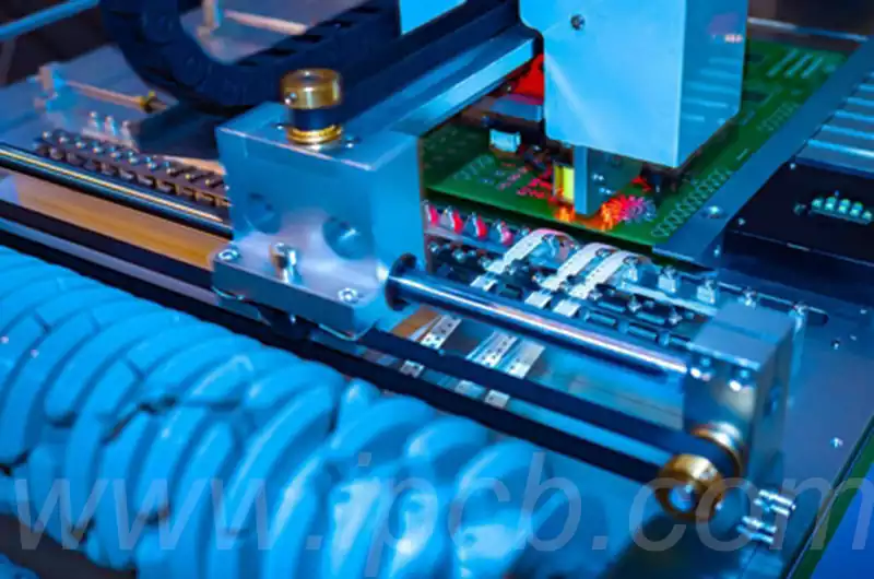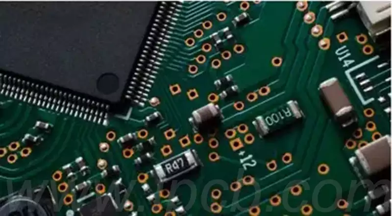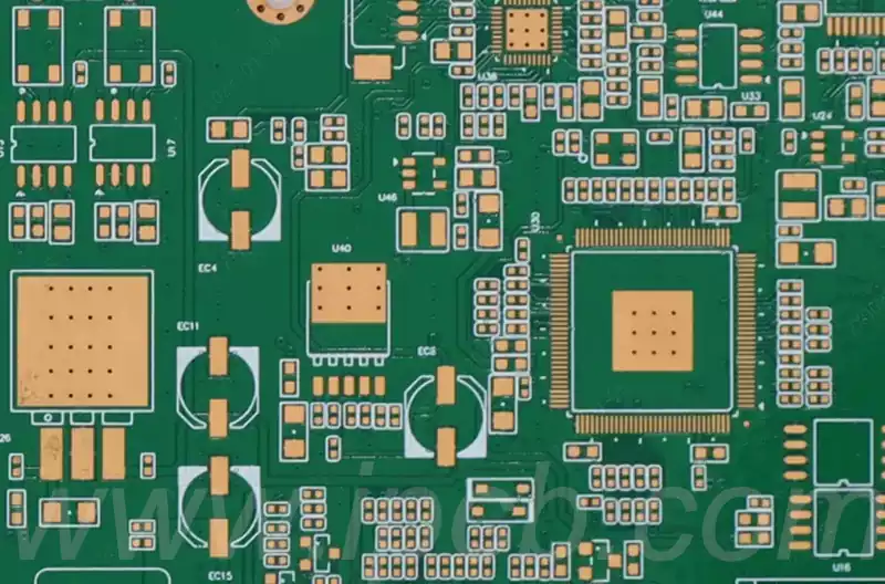
Why preheat before PCBA soldering
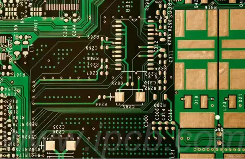
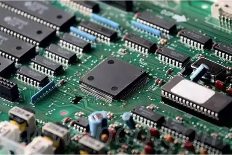
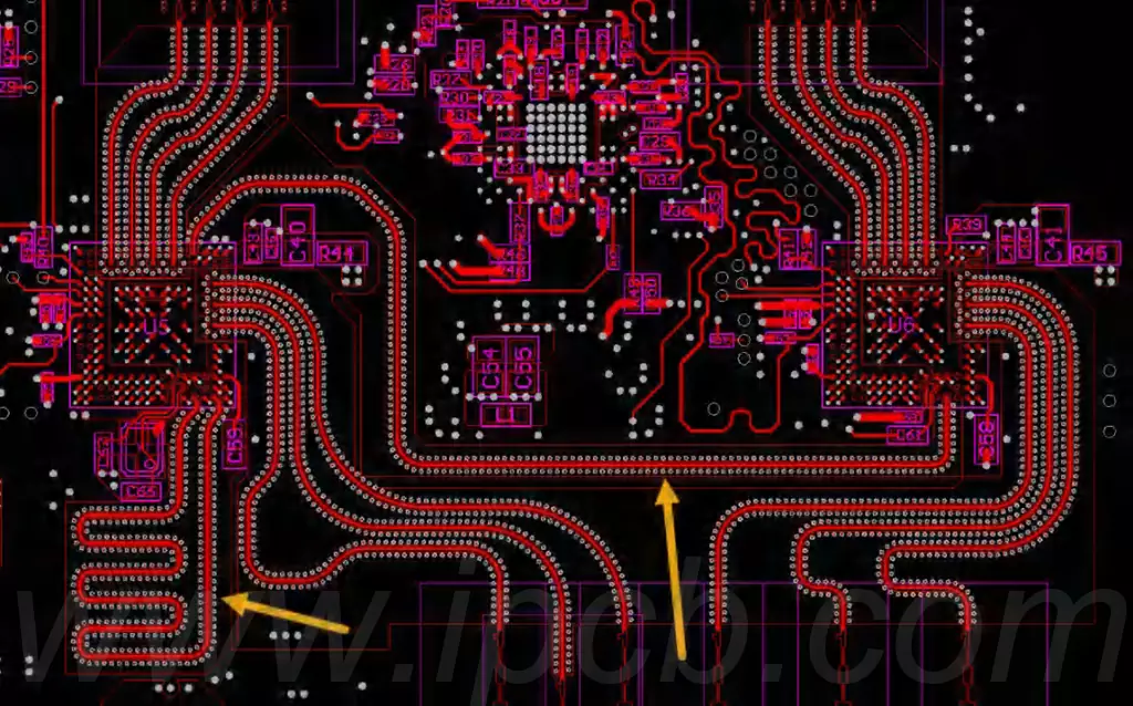
In the pcba assembly process, welding is a key step in connecting various components together. In order to ensure the quality and effect of welding, pcba pre-soldering preheating becomes a link that cannot be ignored. What is PCBA pre-soldering heat?When technicians and practitioners hear the term ‘temperature profile’, smt reflow soldering comes to mind. Along […]