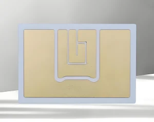
How Millimeter Wave PCBs Enable High Frequency Electronic Applications
Millimeter wave pcbs are specialized circuit boards designed to operate at frequencies of 24 GHz, 28 GHz, 39 GHz, 60 GHz, 77 GHz, 79 GHz, and above. They have become
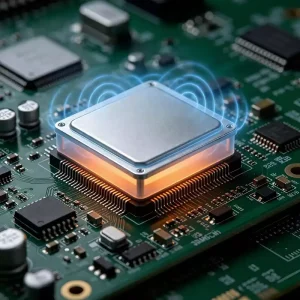
PCB Shielding for High Speed PCB and RF Circuit Design
PCB shielding is an essential design solution in high-speed electronic circuits. As PCB layouts become increasingly compact and integrated, more wireless communication modules—including GPS, Bluetooth, Wi-Fi, and 2G to 5G
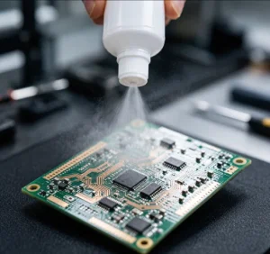
Preventing Electrochemical Migration with pcb board cleaner spray
Deciphering the Underlying Dissolution Mechanism of PCB board Cleaner Spray When a cleaning agent spray is applied to a motherboard that has just undergone a high-heat reflow oven at 260°C,
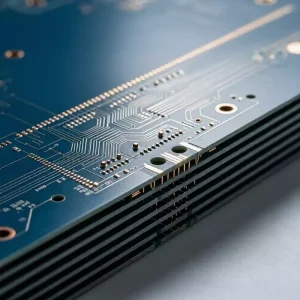
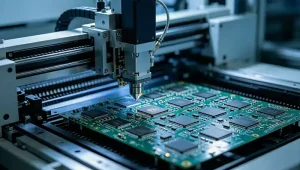
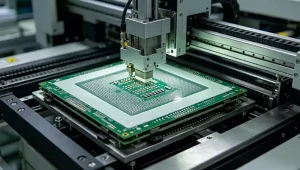
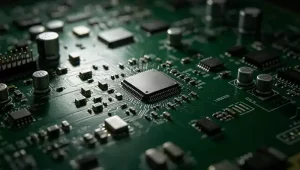
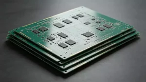
Multilayer PCB Manufacturing Process
Multilayer PCBs are the core foundation of modern high-end electronic equipment, enabling complex circuit routing, high-density signal transmission, and reliable electrical interconnection. Compared with conventional double-sided PCBs, multilayer PCBs feature
Sintering Mechanisms in Thick film circuit boards
Unveiling the Microscopic Topology of Thick-Film Ceramic Substrates Unlike traditional circuit boards manufactured by laminating copper foil, the creation of thick film circuit boards is a magical transformation of inorganic
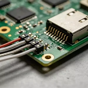
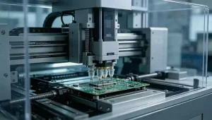
PCB and PCBA Board Connection Methods in Electronics Manufacturing
In today’s electronics manufacturing industry, rigid PCB (Printed Circuit Board) fabrication and PCBA (Printed Circuit Board Assembly) are two indispensable stages in the production of electronic products. A PCB serves
Factors Affecting the Cost of Multilayer PCB Assembly
The final quotation for a multilayer PCB assembly (PCBA) project is never determined by a single manufacturing process. Instead, it is calculated based on a comprehensive evaluation of multiple factors,
SMT Tombstoning Effect Causes Analysis and Effective Prevention Methods
The SMT tombstoning effect is one of the most common structural soldering defects encountered in PCB surface mount assembly, particularly in the production of miniature chip resistors and capacitors. The
Rogers RT duroid 5870 High-Frequency Laminate
Rogers rt duroid 5870 is a high-performance high-frequency laminate that has been trusted by the electronics industry for decades. Manufactured from woven glass fabric reinforced with polytetrafluoroethylene (PTFE), the material
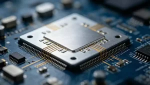
Managing SMT Reliability for Complex pcb board parts
Demystifying the Core Packaging and Thermoelectric Failure of Active Semiconductor Components In the macroscopic layout of PCB board parts, active components are the core brain and power heart of the
Optical Module PCB Ni/Pd/Au Surface Finish
In high-speed optical module packaging, the surface finish applied to the pads of an optical module PCB directly determines wire bonding quality and long-term product reliability. As 100G, 400G, and
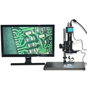
Optimizing Depth of Field in microscope for repair pcb
The Underlying Architecture of Stereo Microscopes and Digital Video Microscopes In the rework workshops of the electronics industry, microscope for repair PCB have undergone a profound technological evolution from traditional
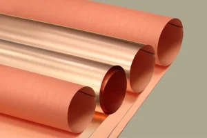
Thermal Management Solutions for copper pcb board
The Powerful Combination of Thermodynamics and Electrical Aspects: Deciphering the Microstructure of Copper-Based Composite Boards In the physical landscape of modern power electronics, high-power energy conversion, and military-grade high-density power
Understanding Multilayer Ceramic Substrates and Their Applications
A multilayer ceramic substrate is a circuit substrate formed by alternately stacking multiple conductive wiring layers and insulating dielectric layers, followed by integrated co-firing into a single structure. Because of
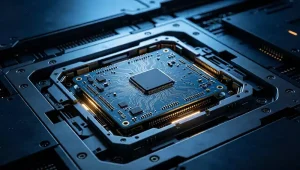
The Role of Anylayer HDI in smartphone pcb
A Macroscopic Glimpse into Microelectronics Physics: Deciphering the Ultra-High-Density Topology of High-Density Mobile Phone Motherboards In the hardware development landscape of modern smartphones and high-end wearable devices, the smartphone PCB
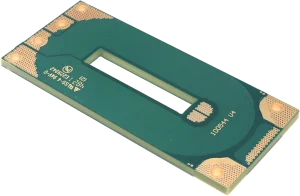
ATE Load Board Design Considerations for High Performance Semiconductor Testing
Among all components within the semiconductor test ecosystem, the ATE Load Board serves as the critical electrical bridge between the tester and the Device Under Test (DUT). While it may
Smartphone PCB Layout Challenges and Design Principles
Smartphone PCB layout is widely regarded as one of the most challenging aspects of product design. Under the dual constraints of ultra-thin form factors and increasingly powerful hardware, designers must
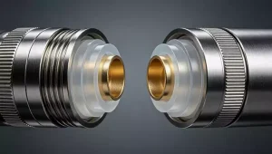
RF Coaxial Connector Structure and Applications
RF Coaxial Connectors (commonly referred to as RF connectors) are precision electromechanical components that integrate both mechanical and electrical functions. They can be assembled onto RF cables, electronic instruments, and
The Impact of pcb circuit board material on Signal Integrity
The Microscopic Electrical Framework: Deciphering the Resin and Matrix Essence of PCB Circuit Board Materials In the vast landscape of the electronics industry, attention is often focused on the intricately
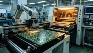
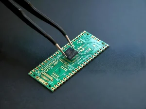
Core FPC SMT Manufacturing Processes and Production Technologies
In FPC manufacturing, Roll-to-Roll (RTR) processing and fixture-mounted assembly represent two fundamentally different production approaches. RTR technology excels in full automation and the manufacture of ultra-thin flexible circuits, while fixture-mounted
Characteristics and Manufacturing Process of High Layer Count PCBs
High layer count pcb, known in the industry as HLC (High Layer Count), are defined as through-hole printed circuit boards with six or more layers. With PCB manufacturing processes continuously
SMT Soldering Quality Assessment and Defect Control
SMT soldering quality is the foundation of electronic assembly reliability. Starting from the appearance criteria of high-quality solder joints, this article systematically analyzes the causes of typical defects such as
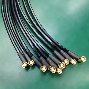
RF Coaxial Cable Structure and Key Performance Characteristics
RF coaxial cable is a specialized transmission medium designed for high-frequency electromagnetic signals. Thanks to its unique coaxial layered structure, it offers key advantages such as stable impedance, excellent shielding
Chip Scale Package (CSP) technology
What Is CSP (Chip Scale Package)?According to the IPC/JEDEC J-STD-012 industry standard, a Chip Scale Package (CSP) is a surface-mount integrated circuit package whose overall package dimensions do not exceed