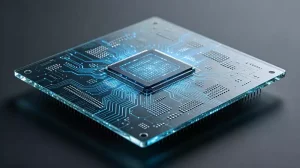
The Principles of Glass Substrates and Their Advantages in AI Chip Industry
What is a glass substrate? Why has it become the core material for advanced packaging in the post-Moore’s Law era? Today, as the computing power of AI chips continues to
Advanced Strategies for Circuit Board Shields
The Microscopic World’s “Breakwater”: Electromagnetic Shielding The Physical Essence of Multilayer Boards In the macroscopic world of modern electronic design, various wireless communication technologies (such as 5G, Wi-Fi 6/7, Bluetooth,
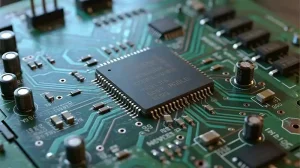
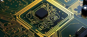
What PCB boards are behind AI computing power?
In the AI computing hardware ecosystem, PCB boards serve as the cornerstone connecting chips to clusters. Whether it’s training large models with hundreds of billions of parameters or performing millisecond-level
The challenges posed by the next generation of optical modules for PCB boards
Optical modules are the core interconnection units in computing infrastructure such as data centres and 5G communications. As optical module speeds rapidly evolve from 100G to 400G, 800G and even
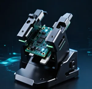
The Importance of pcb circuit board holder in Precision Soldering
“A Rock-Solid ‘Third Hand’: The Mechanical Essence of PCB Board Holders in Manual Soldering” In the R&D, prototyping, and after-sales repair stages of electronic products, although automated surface mount technology
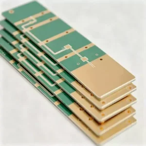
Core Technologies and Applications of High Frequency High Speed Copper Clad Laminates
High Frequency, high speed copper clad laminates (referred to as High Frequency copper clad laminates) are core PCB substrate materials designed for High Frequency signal transmission applications. The core manufacturing
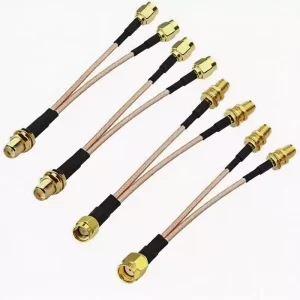
Performance and Selection of RF Cable Assembly
RF cable assembly is essential fundamental transmission components in RF and microwave systems. Their primary function is to enable low-loss, highly stable transmission of RF signals between different devices and
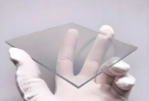
The Role of ITO glass substrate in Optoelectronics
The Paradoxical Unity of Light and Electricity: Deciphering the Physical Essence of ITO Glass Substrates In the world of materials science, “conductivity” and “transparency” are often seen as mutually exclusive
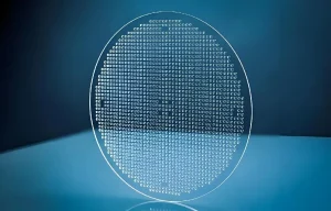
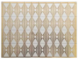
The Advantages of Glass Substrates and Their Manufacturing Processes
With the rapid evolution of 5G/6G communications, optoelectronic displays, high-end microelectronics and aerospace technology, traditional PCB substrates are no longer able to meet the stringent requirements of high-end equipment, such
The Blueprint for Cost Efficient PCB Assembly
Winning at the Starting Line: How to Cut Hidden Costs Through Design for Manufacturability (DFM) In the business world of electronics manufacturing, many clients often focus the majority of their
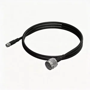
How to choose the right RF test cable
In the wireless communications industry, RF test cables are a core consumable in high-precision test systems, primarily used to connect test instruments to the device under test (DUT) to ensure
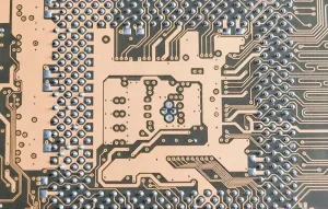
Reasons why PCB multilayer boards are mostly even numbered
PCB circuit boards can be categorised by structure into single-sided, double-sided and multilayer boards. Among these, the design of multilayer boards offers a high degree of flexibility, with no strict
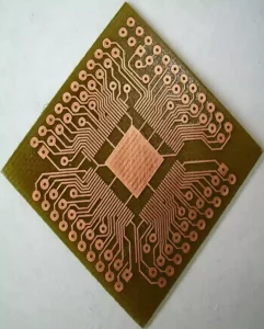
Differences between HDI PCBs and multilayer pcbs
HDI PCB (High-Density Interconnect printed circuit boards) and conventional multilayer printed circuit boards are two types of PCB products in the electronics manufacturing sector that differ significantly in terms of
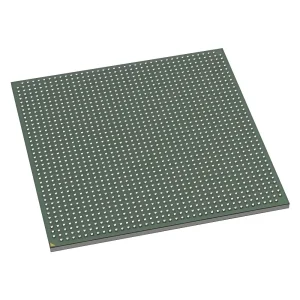
Glass substrates have become the core packaging material for high-performance AI chips
Thanks to their superior physical properties and advantages in large-scale mass production, glass substrates have emerged as the key alternative solution in the advanced packaging sector for next-generation high-bandwidth, high-computing-power
How Intel Glass Substrate Redefines Next-Gen Advanced Packaging
From Organic Resin to Glass: Why Intel Sparked a “Materials Revolution” in Chip Substrates In the history of semiconductor chip development, the renowned “Moore’s Law” has consistently guided the industry’s

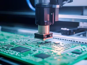
Classification of PCBA Manufacturing Processes and Key Steps
The PCBA manufacturing process encompasses several core stages, including substrate pre-treatment, solder paste printing, component placement, reflow soldering, through-hole insertion, wave soldering, functional testing and final product inspection.The appropriate production
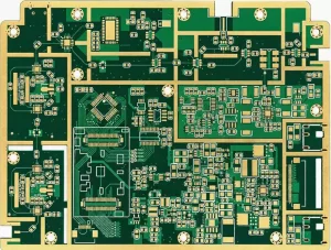
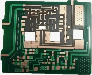
Signal Integrity and Thermal Management Design for AI Server PCBs
As the core component responsible for computing power transmission, signal exchange and power distribution within AI server PCB, high-layer-count, high-performance PCBs directly determine model training efficiency, system stability and data
Key Reliability Strategies for Modern BGA PCB Design
BGA Packaging Pin Evolution and Basic Fan-Out Strategy In the world of modern high-density interconnect circuit board design, BGA PCB design is undoubtedly the ultimate watershed moment testing an engineer’s
The Working Principle of Multilayer Microwave Circuit Boards and Grounding Techniques
Multilayer microwave circuit boards are specialised printed circuit boards designed for high-frequency applications. Through a composite structure of multiple layers of insulating substrate and conductive copper foil, they enable the
Key Considerations for Design for Manufacturability in High-Density BGA PCBs
As the functionality of electronic products continues to evolve, the number of components mounted on PCBs is constantly increasing, component pin pitches are becoming increasingly fine, and circuit design is
Classification and Applications of IC Substrates
As a core foundational material in the high-end chip packaging process, the classification of IC substrates essentially follows a tiered matching principle of ‘material properties → structural form → application
The Performance and Applications of Alumina Ceramic Substrates in RF and Microwave Circuits
In the field of RF and microwave electronics, the performance of substrate materials directly determines the potential for circuit miniaturisation, signal integrity and environmental adaptability. Thanks to its outstanding comprehensive
Post-SMT processes for BGAs
Following surface-mount soldering (reflow soldering), BGA devices typically undergo several post-process steps to enhance their environmental adaptability, mechanical strength and reliability. In accordance with industry practice, these primarily comprise three
The Reflow soldering process
What is reflow soldering? Reflow soldering is a core soldering process in surface-mount technology (SMT), used to establish a mechanical connection and electrical continuity between the terminals or leads of