In modern electronic products, RF PCB design is a core aspect of ensuring device performance and functionality. With the development of wireless communications and Internet of Things (IoT) technologies, the design of RF PCBs has become particularly important, with its complexity and demand for detail increasing day by day.
Layout principles for RF PCB design
- Layout preparation
Before the layout of the RF PCB design, the designer needs to have a detailed understanding of the board’s function, operating frequency band, current and voltage, as well as the main types of RF devices, etc., to clarify the structural design and impedance control requirements. These preparations to ensure the rationality of the design, and lay the foundation for the subsequent layout. - Physical partition
Physical partitioning is the key to layout,the rf pcb design should be based on the signal flow rules to arrange the location of electronic components. For example, components on the RF path should be close to the RF ports and oriented to shorten the length of the RF line as much as possible.At the same time, designers need to consider the mutual interference between different circuits to ensure isolation. - Electrical Partitioning
Electrical partitioning involves separating power,digital and analog signal areas in the layout.When wiring different areas,avoid signal and power lines crossing, which can reduce internal interference.Ensure that circuits accomplishing the same function are arranged in as close an area as possible to reduce the signal loop area. - Alignment Principles
Using the correct alignment is critical, RF alignment should try to go in the surface layer to reduce signal loss. At the same time, long-distance parallel wiring should be avoided, plus ground can effectively reduce the impact of coupling between the signals. In the case of must traverse, should be preferred to use the appropriate cross mode, in order to reduce interference . - Other considerations
In addition, designers should also consider the width of the alignment and mutual distance, such as baseband signal lines should be maintained at an appropriate width to avoid phase errors. Meanwhile, for the VCO control lines, the design should be considered away from the RF signals, which can prevent them from being interfered.
Improve the transmission quality of high-frequency signals in the rf PCB design of the alignment of the way
- Shorten the signal path
When designing a high frequency PCB,the signal path should be shortened as much as possible to reduce the transmission distance of the signal on the board. Shorter paths can reduce signal delay and reflection and improve signal quality. In this regard,reasonable layout planning and routing arrangements are critical. - Limit Lead Turns
When wiring high-frequency circuits,lead turns should be minimized.The use of all straight-line design is the best choice, if you need to turn,you can consider the use of 45-degree fold or arc turn.This approach can reduce the high-frequency signal emission and coupling between each other. - Ensure impedance matching
Good signal impedance matching is crucial for high frequency signal transmission. When the characteristic impedance of the transmission line and the load impedance difference is large, it will cause signal reflection,affecting the signal quality. The impedance of the signal transmission line should be consistent with the load, and in the wiring process should avoid sudden changes. - Alternate interlayer lead minimization
When connecting electronic components, the use of vias should be minimized because each vias introduces additional distributed capacitance, which affects the speed of signal transmission. Appropriately reducing the number of over-holes can help improve the stability of signal transmission. - Maintain signal line spacing
The alignment of high-frequency signal lines should maintain sufficient spacing to minimize the crosstalk phenomenon between signals. Ground wires or ground planes can be inserted between signal lines to isolate them and reduce the possibility of mutual interference. - Use isolated ground lines
When grounding high-frequency digital and analog signals, a high-frequency choke bead or direct isolation should be used to ensure that the two are electrically independent. This can effectively reduce the interference of digital signals on analog signals, thus improving the overall signal quality. - Avoid forming loops
High-frequency signal alignment to avoid the formation of loops, if you can not avoid the loop area should be as small as possible. The smaller the loop area, the smaller the electromagnetic interference generated, which can improve the stability of the signal.
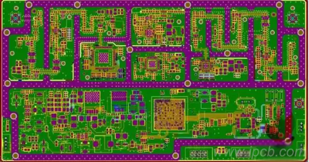
RF PCB stacked design, need to consider a number of factors, including the number of layers, signal type, material selection, impedance control and power and ground plane layout to ensure that the electrical performance and reliability of the circuit.
- Layer Selection
When designing RF PCBs, it is usually recommended to use a stacked configuration of at least four layers. This design can effectively arrange the power and ground layers internally to improve power integrity and signal quality. If the design is for a high-density circuit, more layers may be considered to meet the need for anti-interference between different signals. - Layout of signal layer and ground layer
Signal layer wiring should be routed as close to the ground plane as possible to ensure a complete return path for signals, thus reducing noise and crosstalk. For critical high-speed signal lines, usually using the strip line (Stripline) design, its power and ground plane layer layout should also be closely linked to optimize power distribution and reduce EMI (electromagnetic interference). - Material Selection
Choosing the right material is critical to the performance of the RF PCB.Commonly used materials include FR-4 and Megtron for high-speed applications, which help to reduce losses during signal transmission. In specific scenarios, such as automotive light boards, an aluminum or copper substrate may be required to meet thermal management needs. - Impedance Control
Impedance matching is critical in the RF PCB design process.Mismatched impedance may lead to signal reflection and distortion, thus affecting circuit performance. The design should be through the selection of the appropriate alignment width,spacing and material to control the impedance, usually requires a high degree of positioning accuracy to meet the 50Ω or 100Ω impedance requirements. - Thermal management design
In the design of RF PCB, it is also necessary to consider thermal management. The heat generated by high-power components need to be effectively distributed to avoid damage to the circuit, commonly used solutions include the design of high-power components under the thermal pads and the use of materials with high thermal conductivity. Through thermal simulation, designs can be optimized for effective heat dissipation.
In RF PCB design,proper layout and alignment principles are key to ensuring the quality of high frequency signal transmission. By focusing on details such as pre-layout preparation,physical and electrical partitioning, alignment principles, and stacking design, designers can effectively reduce interference and improve circuit reliability and performance.At the same time, choosing the right materials and performing impedance control are critical to achieving optimal signal transmission. Overall, careful design and optimization not only improves the efficiency of RF circuit boards, but also lays the foundation for the performance of modern electronic equipment.