Unlike standard PCB substrates, the thermal conductivity of PTFE PCBs is not determined solely by the substrate itself, but rather by the combined effects of substrate properties, filler modification, manufacturing processes and application scenarios. The core challenge in optimising thermal conductivity lies in enhancing thermal efficiency without compromising PTFE’s inherent advantages of low high-frequency loss.
PTFE (polytetrafluoroethylene) is hailed as the ‘king of high-frequency’ PCB substrates. Although its intrinsic thermal conductivity of approximately 0.25 W/(m·K) is slightly lower than that of traditional FR-4 substrates (approximately 0.3 W/(m·K)), its excellent dielectric stability, resistance to high and low temperatures, and chemical inertness make it the material of choice for high-frequency, high-speed applications.
Key Factors Influencing the Thermal Conductivity of PTFE PCBs
1.Substrate Molecular Structure: The Foundation of Thermal Conductivity
The main chain of PTFE molecules consists of carbon-carbon single bonds, with fluorine atoms tightly enveloping both sides to form a stable negative charge barrier. Whilst this structure confers excellent dielectric properties and chemical stability, it also results in significant intermolecular thermal resistance, making it difficult for heat to transfer rapidly—this is the intrinsic reason for the relatively low thermal conductivity of pure PTFE substrates.
Heat conduction in pure PTFE relies primarily on molecular thermal motion. The higher the crystallinity, the more ordered the molecular arrangement, the lower the thermal resistance, and the better the thermal conductivity. However, excessively high crystallinity increases the substrate’s brittleness, adversely affecting processability. Therefore, a reasonable balance must be struck between crystallinity and processability.
2.Filler Modification: The Key Method for Enhancing Thermal Conductivity
The thermal conductivity of pure PTFE substrates is limited, making it difficult to meet the demands of high-power applications. By adding highly thermally conductive fillers, thermal pathways can be created within the substrate, reducing thermal resistance and achieving a significant improvement in thermal conductivity. This is currently the most widely used and effective optimisation method in the industry.
Commonly used high-thermal-conductivity fillers are primarily divided into three categories:
Inorganic fillers: such as boron nitride, aluminium oxide, and graphite
Metallic fillers: such as copper powder
Nano-fillers: such as graphene
There are significant differences in the suitability and performance enhancements offered by different fillers; selection must be based on specific application requirements.
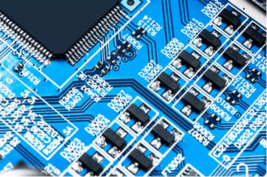
3.Processing Techniques: The ‘Invisible Influencers’ of Thermal Conductivity
Key processes such as drilling, lamination and SMT soldering all directly affect the integrity of the thermal pathways and the interfacial thermal resistance of PTFE PCBs.
Drilling: As the PTFE substrate is soft and has poor thermal conductivity, traditional mechanical drilling can easily lead to heat accumulation, with local temperatures potentially exceeding 260°C. This causes the substrate to soften and stick, disrupting the internal thermal pathways. Additionally, burrs on the hole walls increase interfacial thermal resistance, hindering heat transfer.
Lamination: Improper control of temperature and pressure can result in voids between the substrate and the copper foil, creating thermal resistance barriers that reduce thermal conductivity.
SMT Soldering: Traditional reflow soldering processes are prone to causing localised overheating, with temperature differences of up to 40°C beneath the chip. This not only affects soldering yield but also damages the PCB’s thermal structure.
Furthermore, the surface treatment process of the substrate also affects thermal performance. Enhancing surface roughness through methods such as plasma cleaning can strengthen the bond between the substrate and the copper foil, reduce interfacial thermal resistance, and thereby improve thermal conductivity.
Typical Application Scenarios for PTFE PCB Thermal Conductivity
1.Automotive Millimetre-Wave Radar
Automotive radar typically operates at 77 GHz, with high power density, and must function reliably in extreme environments ranging from -40°C to 125°C. This application places stringent demands on both the thermal conductivity and high-frequency performance of PTFE PCBs, making it one of the core application areas for PTFE PCBs.
2.Aerospace and Satellite Communications
This application places extremely high demands on the thermal conductivity, reliability and environmental resistance of PTFE PCBs. They must operate stably over the long term under extreme temperatures and radiation, placing a heavy reliance on the material’s comprehensive performance.
3.5G Base Stations and High-Frequency Communications
PTFE PCBs are primarily used in core components such as millimetre-wave modules and optical modules. They must simultaneously meet the requirements for low high-frequency loss and moderate thermal conductivity, making them a critical material choice in 5G infrastructure.
The thermal conductivity of PTFE PCBs is determined by the substrate, fillers and manufacturing process. In practical applications, a reasonable balance must be struck between high-frequency performance and heat dissipation requirements.