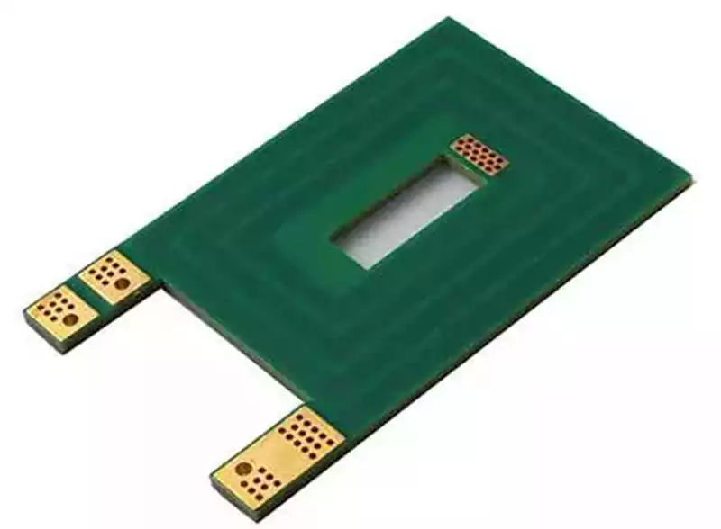
As IC pin densities increase and signal frequencies rise, the choice of PCB surface treatment process has become particularly critical. Gold plated circuit boards were once favoured for their high flatness and long shelf life, but issues such as gold whisker short circuits and the skin effect have become increasingly prominent in high-density, high-frequency applications. Immersion gold boards have therefore emerged as a superior alternative.
Why use gold plated circuit board?
As IC integration continues to advance, the number of pins is increasing and the spacing between them is becoming ever smaller. Traditional vertical tin-spraying processes struggle to flatten densely packed pads, which poses significant challenges for SMT assembly. Furthermore, tin sprayed boards have a short shelf life and are prone to oxidation. In contrast, Gold plated circuit board effectively address these issues:
Superior flatness: In surface mount processes, particularly for ultra-small components such as 0603 and 0402, the flatness of the pads directly affects the quality of solder paste printing, which in turn determines the reliability of reflow soldering. Gold plated circuit boards provide a highly flat pad surface and are therefore widely used in high-density, ultra-small-scale assembly processes.
Longer shelf life: During the prototyping phase, due to unpredictable component lead times, PCBs often need to be stored for several weeks or even one to two months before soldering can commence. Gold plated circuit boards have a significantly longer shelf life than lead-tin alloy boards, and their cost during the prototyping stage is virtually identical to that of lead-tin alloy boards; consequently, they are favoured by engineering and procurement personnel.
However, as routing density has increased further, with line widths and spacing reduced to 3–4 mils (approximately 0.076–0.1 mm), the drawbacks of Gold plated circuit boards have gradually become apparent:
Risk of gold whisker short circuits: In high-density routing, the gold layer may form fine metal whiskers or residues, leading to micro-short circuits.
Skin effect impacting signal quality: At high frequencies, current tends to flow concentrated on the surface of the conductor (the skin effect). The surface of Gold plated circuit boards typically consists of a multi-layer structure, such as nickel-gold. When high-frequency signals propagate across the interfaces between different plating layers, additional losses and distortion occur, severely compromising signal integrity.
Why use electroplated gold boards?
To overcome the aforementioned shortcomings of gold plated circuit board, the electroplated gold process (electrolytic nickel-gold) was developed. Electroplated gold boards possess the following notable characteristics:
Superior appearance: The crystal structure formed by electroplated gold is denser and more uniform than that of plated gold, presenting a more vibrant golden hue and resulting in higher customer satisfaction.
Better soldering performance: The crystal structure of the electroplated gold layer facilitates solder wetting and diffusion, minimising the risk of soldering defects and preventing customer complaints.
Superior high-frequency signal transmission: The nickel gold layer is deposited only on the pads, whilst the copper layer on the traces comes into direct contact with the solder mask. The skin effect of high-frequency signals is primarily transmitted through the copper layer, unaffected by the gold layer, resulting in better signal integrity.
Strong resistance to oxidation: The crystal structure of the electroplated gold layer is denser with lower porosity, making it less prone to oxidation and ensuring long-term reliability.
No risk of gold filament micro-short circuits: As the gold plating is confined to the pad areas, there is no excess gold layer between the traces, thereby eliminating the risk of gold filament short circuits.
Stronger solder mask adhesion: The copper layer on the surface of the traces bonds directly with the solder mask ink, resulting in far superior adhesion compared to Gold plated circuit board(where the solder mask must be applied over a nickel-gold layer, making it prone to peeling).
Compensation does not affect spacing: When line width compensation is applied during engineering, the immersion gold does not alter the line thickness, thus preventing a reduction in spacing, which is beneficial for high-density routing.
Controllable stress, beneficial for bonding: The internal stress of the immersion gold layer is low and uniform, resulting in more stable processing for products requiring gold wire bonding. However, it should be noted that the electroplated gold layer is softer than the electroplated gold layer, resulting in a shorter service life when used in wear-resistant applications such as gold fingers.
Flatness and shelf life: The pad flatness and shelf life of electroplated gold boards are comparable to those of electroplated gold boards, fully meeting the requirements of modern SMT and long-term storage.
Immersion Gold vs. Electroplated Gold
In practice, gold plating processes are divided into two types: electroplated gold and immersion gold (chemical nickel-gold/chemical immersion gold). In terms of soldering performance:
The crystal structure of electroplated gold layers is relatively loose and contains micro-pores, which can easily lead to poor solder wetting and affect soldering quality.
Immersion gold layers are dense and uniform, offering excellent solderability.
Consequently, unless a product has specific requirements such as bonding or wear resistance for gold fingers, most PCB designs currently prioritise the immersion gold process. Common PCB surface treatment methods include: gold plating (electrolytic gold/immersion gold), silver plating, OSP, tin plating (lead-free/lead-free), and rosin coating for paper based substrates.
Gold plated circuit boards are suitable for gold fingers or bonding applications requiring high wear resistance, whilst electroless gold plated circuit boards offer comprehensive advantages in terms of solderability, signal integrity and reliability, and have become the mainstream choice for high-density, high-frequency PCBs.