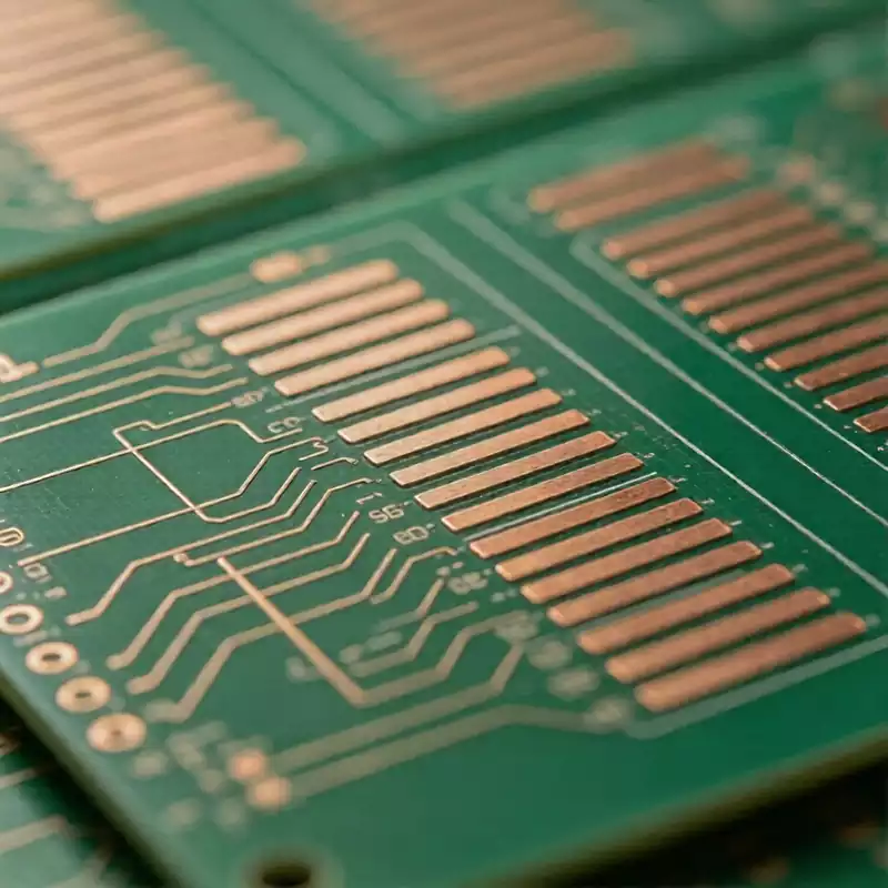
PCB etching is the core process for PCB circuit pattern formation and one of the most critical manufacturing technologies used in printed circuit board fabrication. By selectively removing unwanted copper, the etching process accurately transfers the designed circuit pattern onto the copper-clad laminate, ensuring dimensional accuracy, conductor integrity, and overall PCB performance. Today, PCB etching has become one of the most widely adopted and indispensable processes in PCB manufacturing.
PCB etching is a precision photochemical manufacturing process based on photolithography technology. Its fundamental principle is to transfer the circuit pattern by utilizing the photosensitive characteristics of dry film photoresist. During production, a photosensitive resist is uniformly laminated onto both sides of the copper-clad substrate. Through UV exposure using a phototool, the designed circuit artwork is accurately transferred onto the photoresist layer.
After the development process, the unexposed photoresist is removed, exposing the unwanted copper areas while leaving the circuit pattern protected by the developed resist. The exposed copper is then chemically dissolved by the etchant, whereas the copper protected by the photoresist remains intact. After etching, the remaining dry film resist is stripped, leaving a complete, high-precision PCB circuit pattern with accurate conductor geometry and consistent trace spacing.
The essence of PCB etching is a controlled oxidation-reduction reaction that selectively removes exposed copper foil. To ensure process stability, the entire etching process is carried out under a tightly controlled temperature environment, typically maintained between 40°C and 50°C. During production, an automated spray etching system uniformly sprays the qualified etchant onto the copper surface.
Copper areas not protected by the etch resist react with the etchant and are gradually dissolved, while the copper traces protected by the dry film remain unaffected, exposing only the substrate in the etched areas. After the etching process is completed, the remaining dry film resist is removed using a dedicated stripping process, producing clean, well-defined PCB circuitry.
The etching solution is a chemically balanced multi-component system consisting primarily of cupric chloride (CuCl₂), hydrogen peroxide (H₂O₂), high-purity hydrochloric acid (HCl), and softened deionized water. The concentration and purity of each chemical component must be maintained within strict process specifications, as any deviation may directly affect etching accuracy, sidewall quality, and overall PCB manufacturing quality.
Because the etching process directly determines circuit pattern accuracy and electrical performance, it is one of the most critical quality control stages in PCB fabrication. The following process control requirements must be strictly implemented to prevent manufacturing defects.
Key Quality Control Requirements
Eliminate residual copper.
No unwanted copper residue is permitted on the PCB surface, particularly in narrow trace spacing, multilayer panel recesses, or other difficult-to-etch areas. Residual copper may cause electrical shorts, current leakage, or circuit malfunction.
Completely remove residual dry film resist.
No photoresist residue should remain on the board surface or around pad edges after stripping. Residual resist may result in localized exposed copper, poor plating adhesion, coating delamination, copper oxidation, and long-term reliability issues.
Precisely control the etching rate.
The etching speed shall be optimized according to copper thickness and circuit design requirements. Over-etching must be prevented because it can reduce trace width, increase conductor spacing, and degrade dimensional accuracy. Trace width tolerance and conductor pitch are critical quality control parameters and should be continuously monitored throughout production.
Maintain dry film integrity during etching.
The dry film resist protecting the circuit pattern must remain intact throughout the spray etching process. Peeling, cracking, blistering, or lifting of the resist can expose protected copper and lead to defective circuitry.
Maintain a clean and defect-free board surface.
After etching and resist stripping, the PCB surface shall be free from oil contamination, chemical residue, dust, and foreign particles. Physical defects such as copper lifting, blistering, scratches, or mechanical damage are unacceptable.
Control panel handling and conveyor operation.
Conveyor speed, board orientation, and panel spacing should be properly controlled during loading and transport to prevent panel jamming or prolonged dwell time inside the etching chamber, which may result in uneven etching, excessive oxidation, or localized over-etching.
Ensure uniform spray distribution.
Spray nozzles should be regularly inspected and calibrated to ensure uniform etchant distribution across both sides of the PCB and throughout the entire panel surface. Uniform spray coverage is essential for preventing localized under-etching, over-etching, and asymmetric circuit formation.
Critical Process Parameters for PCB Etching
The stability of the PCB etching process depends on precise control of process parameters, including solution chemistry, operating temperature, equipment condition, and conveyor settings. Typical process specifications are as follows:
| Parameter | Recommended Specification |
|---|---|
| Etchant operating temperature | 40–50°C (Recommended: 45°C) |
| Hydrogen peroxide (H₂O₂) concentration | 1.95–2.05 mol/L |
| Dry film stripper operating temperature | 50–60°C (Recommended: 55°C) |
| Maximum safe operating temperature of the etching machine | ≤55°C |
| PCB drying temperature | 70–80°C (Recommended: 75°C) |
| Panel spacing on conveyor | 5–10 cm to ensure sufficient spray coverage and chemical reaction time |
| Cupric chloride solution specific gravity | 1.20–1.30 g/cm³ |
| Hydrochloric acid (HCl) concentration | 1.90–2.05 mol/L |
| Additional control items | Panel loading angle, conveyor guide flatness, upper and lower spray nozzle operation, and spray pressure |
Maintaining these parameters within their specified process windows is essential for achieving consistent etching performance, minimizing side etching (undercut), ensuring dimensional accuracy, and producing high-quality PCB circuitry with excellent manufacturing yield and long-term reliability.
PCB Etching Process Flow
(1) Dry Film Stripping
Dry film stripping (D/F removal) is an essential pretreatment process performed before and after PCB etching. It is primarily applied at two critical stages of PCB fabrication: the removal of dry film resist after inner-layer circuit etching, and the stripping of dry film before outer-layer negative-pattern etching. The stripping process is well established and highly automated, with most PCB manufacturers employing horizontal conveyorized stripping equipment. The stripping solution is typically an alkaline solution based on sodium hydroxide (NaOH) or potassium hydroxide (KOH), with a concentration maintained between 1% and 3%.
To ensure complete dry film removal and stable process performance, the following process control measures should be implemented.
After exposure and curing, the dry film resist partially dissolves and partially peels away in the alkaline stripping solution. Therefore, the efficiency of the filtration system is critical. The filtration system should be cleaned and maintained regularly to prevent residue accumulation, which can reduce stripping efficiency and contaminate the stripping solution.
To eliminate residual dry film remaining along circuit edges, most stripping systems are equipped with auxiliary cleaning mechanisms such as soft brushing or ultrasonic agitation. These features effectively remove resist residues that may become partially encapsulated by secondary copper plating, making them particularly effective during dry film stripping after outer-layer etching. Some production processes previously incorporated BCS (Butyl Cellosolve) as a stripping accelerator to improve resist dissolution. However, because BCS does not comply with current environmental regulations and poses health risks to operators, its use has been gradually phased out across the PCB industry.
Because potassium ions in potassium hydroxide solutions may attack the tin or tin-lead etch resist, the stripping chemistry used before outer-layer etching must be carefully selected. After stripping, the PCB panels should be thoroughly rinsed with deionized water. Many production lines also incorporate acid neutralization and anti-oxidation treatments to eliminate alkaline residue, prevent copper oxidation, and improve subsequent process reliability.
(2) Circuit Etching
Circuit etching is the core process for PCB pattern formation, selectively removing unwanted copper through precisely controlled chemical reactions. The etching mechanism, equipment configuration, chemical management, and preventive maintenance all have a direct impact on dimensional accuracy and product quality.
1.Copper Etching Mechanism
In an alkaline etching system, dissolved copper ions readily form copper hydroxide precipitates, which reduce etching efficiency and contaminate the etching solution. To prevent this, a sufficient amount of aqueous ammonia is added to the etchant, allowing stable cupric ammine complexes to form and suppress precipitation.
The cupric ammine complex acts as an oxidizing agent that continuously oxidizes and dissolves metallic copper on the PCB surface. During the reaction, cuprous ions (Cu⁺) are produced as intermediate products with very low solubility. These cuprous ions are continuously oxidized by ammonia, ammonium ions, and oxygen supplied from the surrounding air, converting them back into soluble cupric ions (Cu²⁺) that re-enter the etching cycle. As copper concentration gradually increases, the oxidation capacity of the etchant decreases, resulting in a reduction in etching efficiency.
For this reason, the exhaust ventilation system of the etching machine serves not only to remove ammonia vapor but also to introduce fresh air, supplying sufficient oxygen to accelerate the oxidation reaction and maintain a stable copper etching rate.
To further improve etching performance, modern alkaline etchants typically contain various proprietary additives. Accelerators enhance oxidation efficiency and suppress cuprous ion precipitation. Anti-undercut additives minimize lateral etching (side etching), resulting in straighter conductor sidewalls and improved line definition. Volatility suppressants reduce ammonia evaporation at elevated operating temperatures while preventing copper precipitation, thereby maintaining long-term chemical stability of the etching solution.
2.Equipment Optimization and Process Design
To increase production throughput, alkaline etching systems are commonly operated at temperatures above 48°C. Elevated temperatures improve the copper dissolution rate but also accelerate ammonia evaporation, producing strong odors. Consequently, an appropriately sized exhaust system is required to maintain a safe working environment.
However, excessive exhaust airflow removes excessive amounts of active ammonia from the etching solution, increasing chemical consumption and production costs. Therefore, throttle valves or airflow control devices are typically installed within the exhaust duct to optimize ventilation while minimizing ammonia loss.
Etching uniformity is often affected by the so-called “water pooling effect.” Residual water remaining on the PCB surface after previous processes can prevent fresh etchant from contacting the copper surface, causing localized over-etching at the leading edge of the panel and non-uniform etching across the board.
To minimize this phenomenon, modern PCB etching equipment incorporates several optimized design features. Panels are typically conveyed with the fine-line side facing downward and the coarse-line side facing upward to improve etching uniformity. Independent adjustment of the upper and lower spray nozzle pressures compensates for etching differences between the two panel surfaces. High-end spray etchers may also employ delayed activation of the leading spray zone during panel entry to improve chemical distribution. Some advanced manufacturers have adopted vertical spray etching systems, which effectively eliminate etching differences between the top and bottom surfaces of the PCB while significantly improving overall process consistency.
3.Automatic Chemical Replenishment Control
Modern PCB production lines utilize automatic ammonia replenishment systems to maintain stable etchant chemistry. The system continuously monitors the specific gravity of the etching solution using a high-precision density meter combined with temperature compensation, eliminating measurement errors caused by temperature fluctuations.
Upper and lower control limits for solution specific gravity are programmed into the control system. When the measured value exceeds the upper limit, ammonia is automatically added until the specific gravity returns to the preset lower limit, where replenishment is automatically stopped.
To ensure accurate chemical control, the locations of the specific gravity sensor and the chemical injection point must be carefully calibrated. Improper positioning may introduce measurement delays, leading to excessive ammonia addition, solution overflow, unnecessary chemical consumption, and unstable process control.
4.Preventive Maintenance of Etching Equipment
Routine preventive maintenance is essential for maintaining stable etching quality and maximizing equipment reliability.
The pH value of the etching solution should be monitored regularly to prevent abnormal chemical conditions that may produce light-blue cuprous sludge, resulting in reduced etchant activity and circuit contamination.
Spray nozzles should be inspected and cleaned daily to ensure unobstructed spray patterns and uniform chemical distribution. A high-efficiency filtration system should be maintained to prevent particulate contamination from clogging the spray nozzles.
The automatic specific gravity monitoring and chemical replenishment system should also be calibrated periodically to ensure accurate concentration measurement and chemical dosing. Stable control of solution chemistry is essential for maintaining consistent etching performance, minimizing dimensional variation, and achieving high manufacturing yields.
(3) Tin or Tin-Lead Resist Stripping
During outer-layer PCB fabrication, the electroplated tin or tin-lead layer serves solely as an etch resist, protecting the underlying copper circuitry from chemical attack during the etching process. It provides no functional value in the finished PCB. Therefore, once etching is complete, the protective metal layer must be completely removed. Inadequate stripping control can lead to circuit defects, reduced product reliability, and increased manufacturing costs.
Today, the PCB industry primarily uses commercial tin and tin-lead stripping chemistries, which are generally classified into single-component and two-component systems. Depending on the stripping mechanism, these formulations can also be categorized as complete-dissolution or partial-dissolution processes. Common chemical systems include fluoride–hydrogen peroxide formulations and nitric acid–hydrogen peroxide formulations, among others.
Regardless of the formulation used, tin or tin-lead stripping processes present several potential challenges:
Excessive chemical attack on the exposed copper circuitry, resulting in copper surface damage.
Incomplete removal of the tin or tin-lead resist layer, leaving metallic residues that may affect subsequent processing and electrical reliability.
Difficult treatment and disposal of spent stripping solutions, leading to increased environmental compliance requirements and waste treatment costs.
To ensure a stable and reliable stripping process, manufacturers must optimize equipment operating parameters, precisely control the thickness and uniformity of the plated tin or tin-lead etch resist before stripping, and regularly monitor the effectiveness of the stripping solution, replacing it at appropriate intervals to maintain consistent stripping performance and prevent process-related defects.
After the tin or tin-lead stripping process is completed, the outer-layer circuitry is fully formed. A 100% visual inspection should then be performed to verify circuit integrity and identify any manufacturing defects, including incomplete stripping, conductor damage, over-etching, under-etching, or other pattern-related abnormalities.
Future Development of PCB Etching Technology
As electronic products continue to evolve toward miniaturization, lightweight construction, and high-density integration (HDI), PCB circuit patterns are becoming increasingly finer, via diameters are shrinking, and circuit layouts are becoming more densely packed. These trends place significantly higher demands on the precision and uniformity of conventional etching processes.
To meet these challenges, stricter process control is required throughout PCB manufacturing, including tighter control of etchant chemistry, higher equipment automation accuracy, optimized process parameter management, and more comprehensive quality assurance systems. Maintaining dimensional accuracy, minimizing side etching (undercut), and ensuring consistent etching performance across increasingly complex PCB designs have become critical manufacturing objectives.
Looking ahead, the development of PCB etching technology will continue to focus on higher precision, greater automation, improved process stability, and intelligent manufacturing. Advanced chemical control systems, real-time process monitoring, automated equipment optimization, and digital quality management will play increasingly important roles in achieving higher production yields, tighter dimensional tolerances, and superior PCB reliability for next-generation electronic products.