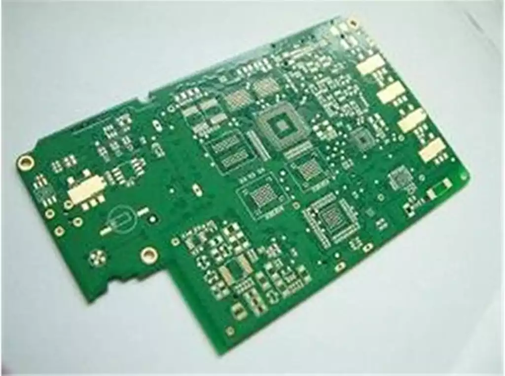
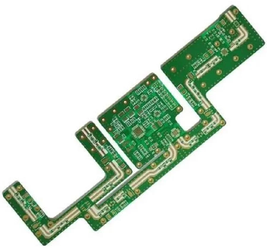
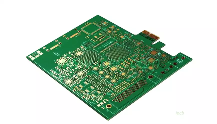
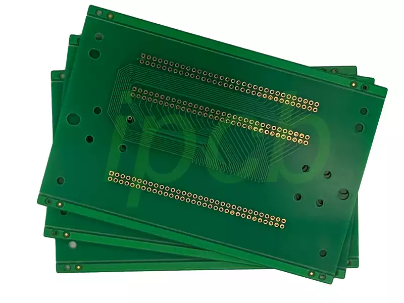
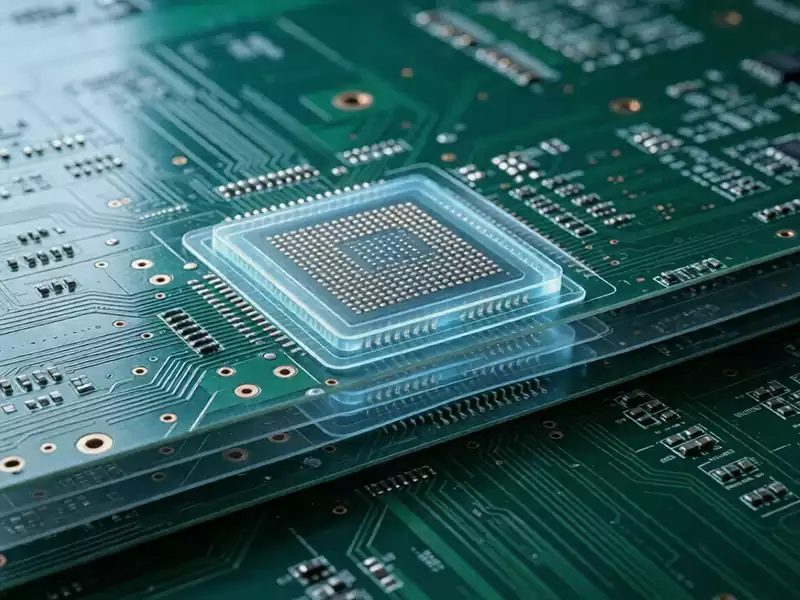
As the number of chip I/O pins increases dramatically, conventional single layer and double layer PCBs no longer provide sufficient routing space to fan out the inner rows of BGA pads. With their superior routing capacity and stacked layer architecture, multilayer PCBs have become the primary solution for high density package routing challenges and now serve as the mainstream platform for high speed PCB design.
At the same time, electronic systems have entered the era of high speed data transmission, where high frequency signal applications are becoming increasingly common. Modern PCB design is no longer limited to simply providing electrical connectivity. By combining multilayer PCB structures with advanced transmission line design techniques, engineers can optimize electrical interconnect performance while maintaining cost effective manufacturing, achieving an optimal balance between high speed circuit performance and production cost.
The primary objective of high speed PCB design is to optimize signal integrity (SI). Designers must effectively address signal reflection, crosstalk, propagation delay, and simultaneous switching noise (SSN), all of which can lead to signal distortion, unstable transmission, and degraded overall system performance if not properly controlled.
Transmission line technology has a long development history. The coaxial transmission line, invented by Oliver Heaviside, was the earliest standardized transmission structure and was originally developed to reduce signal attenuation in long distance telegraph communication. In modern PCB design, however, microstrip and stripline have become the two dominant transmission line structures supporting high speed signal transmission.
Both mainstream PCB transmission line structures were developed during the 1950s. Stripline was introduced by Robert M. Barrett as a dielectric transmission structure operating in the transverse electromagnetic (TEM) mode. Approximately two years later, ITT Laboratories introduced the microstrip transmission line, establishing two complementary transmission line technologies that remain widely used today.
Their structural differences result in significantly different electrical characteristics. A microstrip is routed on the outer layer of the PCB and is directly exposed to the surrounding environment. Consequently, its electromagnetic fields are more likely to radiate outward, creating electromagnetic compatibility (EMC) concerns while also making the signal more susceptible to external interference. Even slight variations in the dielectric constant of the solder mask can alter the characteristic impedance of a microstrip, negatively affecting signal transmission stability.
Because of these limitations, the PCB industry has established a widely accepted design practice: critical high speed signals should be routed on internal stripline layers whenever possible. Embedded between dielectric layers and shielded by reference planes above and below, stripline provides highly stable impedance, lower electromagnetic radiation, and superior immunity to external interference.
The widespread adoption of multilayer PCB technology has further improved the transmission environment for high speed signals and has become the foundation of modern high speed circuit design. Dedicated power and ground planes not only provide substantially greater routing capacity and flexibility but also establish reliable electromagnetic shielding and low impedance return paths. This effectively suppresses crosstalk and electromagnetic radiation while continuing to drive PCB technology toward higher layer counts and greater circuit density.
As semiconductor process technologies continue to scale down, digital signal edge rates have become significantly faster, resulting in higher harmonic content and making transmission line effects increasingly critical. Traditional PCB design approaches that focus solely on electrical connectivity are no longer adequate for today’s high speed electronic systems.
Modern PCB routing must accurately control electromagnetic wave propagation characteristics to prevent signal distortion and maintain signal integrity while ensuring compliance with EMC requirements. Due to inherent structural limitations, single layer and double layer PCBs cannot provide sufficiently stable transmission line structures for high speed applications. Consequently, four layer, six layer, and other multilayer PCB configurations have become industry standards. Their multilayer architecture enables critical high frequency signals to be routed as internal striplines, providing low loss, highly stable signal transmission.
In practical high density multilayer PCB manufacturing, material selection and fabrication processes directly determine product performance and manufacturing yield. Six layer PCBs are commonly used for high integration packages such as BGA and QFN, while surface mount technology (SMT) requires exceptional PCB surface flatness. Electroless Nickel Immersion Gold (ENIG) provides a flat and uniform pad surface with excellent solderability, making it particularly well suited for high density multilayer PCBs and significantly reducing soldering defects such as cold joints and insufficient solder wetting.
Via in pad technology is one of the most important routing optimization techniques for multilayer PCB design, allowing the routing density advantages of multilayer structures to be fully realized. Because vias are integrated directly into component pads, this technology eliminates the need to consume valuable surface routing space for conventional fan out vias, substantially increasing routing density on the outer layers.
Furthermore, power and ground pads can connect directly to their corresponding power and ground planes through embedded vias, eliminating the parasitic inductance associated with traditional trace connections. This optimizes the power distribution network (PDN), improves power integrity (PI), and enhances the overall electrical performance of high density multilayer PCBs.