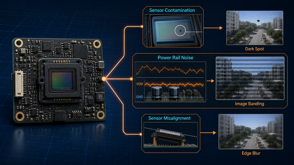
A camera PCB board can pass AOI, electrical testing and firmware programming while still producing an unacceptable image. Sensor contamination, mounting deviation, power-rail noise and optical misalignment may remain invisible until the assembled board is connected to a lens and operated as a complete imaging system.
This is the central manufacturing challenge for surveillance cameras, video doorbells and other security products. These projects often combine multiple product variants, frequent engineering changes and moderate volumes with strict requirements for image consistency and outdoor reliability.
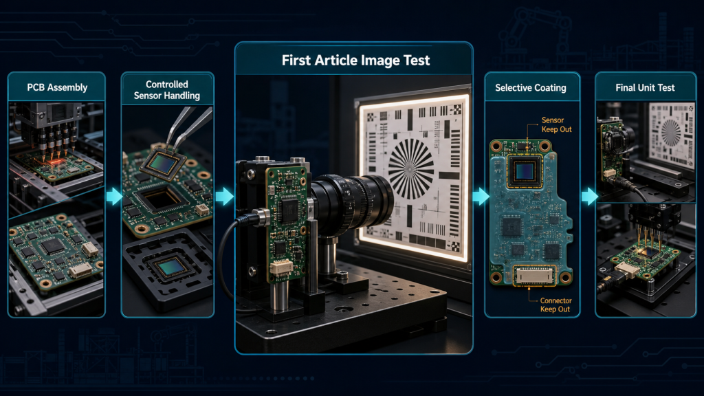
A manufacturing partner supporting a camera PCB board must therefore connect PCB assembly, sensor handling, optical verification and final product testing within one controlled production process. The supplier also needs enough flexibility to manage pilot runs without losing the documentation and process discipline required for larger batches.
Why Camera Electronics Require Different Manufacturing Controls
An IP camera mainboard combines several electrical domains in a limited area. The image sensor requires stable, low-noise power, while the processor and memory generate fast digital transitions. Ethernet, MIPI CSI-2 or another video interface carries high-speed data. PoE conversion, infrared illumination, motor control and audio circuits can introduce switching noise and sudden load changes.
These circuits may operate correctly when tested individually but interact poorly at the system level. Ripple coupled into the image sensor’s analogue supply can appear as fixed-pattern noise, horizontal bands or degraded low-light performance. Poor return-path control around a high-speed interface may not prevent startup, but it can reduce signal margin and cause intermittent frame errors.
Image sensor manufacturers specifically warn that CMOS sensors are sensitive to electromagnetic interference, substrate coupling, thermal noise and power-supply ripple. Noise on the analogue supply can directly influence image quality, which means power integrity must be treated as an imaging requirement rather than only as a voltage measurement. onsemi image sensor power and clocking design note
The power architecture of an IP camera is also more complex than that of a conventional control board. Separate rails may supply the sensor core, sensor I/O, analogue imaging circuits, processor, DDR memory, Ethernet PHY, audio section and infrared illumination. TI’s IP network camera reference design illustrates this multi-rail structure and includes transient protection at the power input. TI IP network camera power reference design
These electrical interactions mean that manufacturers must evaluate the camera PCB board as part of an imaging system rather than simply as an assembled circuit board.
Why Electrical Tests Can Miss Image Defects
One of the largest production risks occurs when a process remains electrically acceptable but changes the optical output of an entire batch. AOI can confirm component presence and solder-joint appearance, while functional testing can verify startup and communication. Neither test automatically detects dust on the sensor, insufficient focus travel or image noise that appears only in night mode.
Sensor contamination can survive normal inspection
The image sensor is one of the most contamination-sensitive components in a security camera PCB assembly. A particle on the sensor cover glass can create a fixed dark mark in the image. Flux residue, cleaning residue or volatile contamination may produce haze that becomes more visible under strong illumination or after the camera has operated for an extended period.
Correcting contamination after lens installation is expensive. The product may need to be opened, cleaned, refocused and resealed. The resulting work affects the complete optical assembly rather than only the PCBA.
Sensor cleanliness should therefore be controlled after soldering, before lens installation and immediately before the optical assembly is closed. Waiting until final image testing to identify particles allows the defect to move too far through production.
Image sensor handling must also be defined as a controlled process. The cover glass should be protected from flux, particles and unnecessary physical contact. onsemi recommends controlling particulate contamination, using ionized air appropriately and avoiding cleaning agents that can damage the cover glass, resin, sealant or optical coatings. Its guidance also notes that devices containing color filter arrays and microlenses may be sensitive to excessive soldering heat. onsemi image sensor handling guidance
Protection methods require ESD consideration as well. Applying or removing unsuitable tape directly from the sensor glass can generate electrostatic charge and produce optical artifacts. Suitable handling procedures include grounded working surfaces, ESD-compatible gloves, controlled ionized airflow and periodically verified protection measures. onsemi trapped-charge handling guidance
Sensor position affects the optical result
A sensor can be electrically functional while being mechanically misaligned. Angular deviation may create a tilted image plane, while an incorrect sensor-to-lens distance can reduce the available focus range or cause edge blur.
AOI does not prove that the complete optical path will focus correctly. Dimensional inspection can control placement position and package height, but it cannot replace a powered image test using the intended lens arrangement.
The mechanical relationship between the lens holder, sensor package and camera PCB board should be checked during first-article production. The assembly is powered and used to capture a defined target so that image orientation, focus travel, center-to-edge sharpness and fixed contamination marks can be evaluated before the complete batch is released.
This test should not depend on an operator’s personal judgment. Target distance, illumination, lens position, image acceptance criteria and recorded results must be included in the process documentation. If the sensor package, stencil, placement program, lens holder or reflow profile changes, the first-article optical check should be repeated.
Power noise may appear only in difficult scenes
A camera can produce a normal image under bright laboratory lighting while showing noise in night mode. Low-light operation uses higher gain and longer exposure, making sensor power noise and grounding weaknesses easier to see.
Power verification should include more than nominal voltage. Ripple, load-transient response, rail sequencing and the relationship between analogue and digital sensor supplies should be evaluated under realistic operating modes.
Infrared LEDs are particularly important. Switching the illumination on can create a sudden load change and inject current into shared power or ground paths. PTZ motors, audio amplifiers and mechanical IR-cut filters can produce similar disturbances. Testing only an idle camera may miss image interference that appears during normal operation.
TI and onsemi camera reference designs use dedicated low-noise supply arrangements for image sensors. These designs demonstrate why supply noise should be addressed during schematic design, PCB layout and prototype validation instead of being treated as an image-tuning problem after production. TI low-noise CMOS image sensor supply design
Moving from Pilot Runs to Repeatable Production
A small pilot batch proves that the design can be assembled, but it does not automatically prove that the process is ready for volume production.
During prototyping, experienced technicians can compensate for incomplete work instructions. They may inspect the sensor manually, adjust the lens several times or correct a coating mask by hand. These actions can produce acceptable samples while hiding a process that cannot be repeated efficiently across hundreds or thousands of units.
Before the production quantity increases, manual judgment needs to become a controlled parameter. Sensor handling requires defined environmental and ESD conditions. Lens installation needs controlled positioning and retention. Focus adjustment requires a test target and acceptance window. Firmware, calibration data and hardware revision must remain linked through batch or serial-number records.
Effective revision control must also prevent materials, firmware and placement programs intended for different versions of a camera PCB board from entering the same batch. A sensor or lens change can affect the stencil, placement program, firmware, calibration file, test fixture and packaging label at the same time.
This is particularly important for security products because several similar models may run in parallel. Two boards may look nearly identical while requiring different sensors, infrared settings or firmware packages. Visual recognition by an operator is not a reliable version-control method.
A stable transition is easier when pilot and production teams follow the same controlled documentation. Equipment may change as volume increases, but image-quality criteria, process revision records and test limits should remain consistent.
Controlling Conformal Coating Around Camera Components
Outdoor security products may require conformal coating to reduce the effects of humidity, condensation and contamination. In these assemblies, the camera PCB board normally contains more coating keep-out areas than a conventional outdoor control board.
The image sensor and lens-mounting region must remain optically clean. Connector contacts, microphone openings, pressure sensors, programming interfaces and selected thermal surfaces may also require protection from coating. Material beneath a processor heat-transfer pad can interfere with the intended thermal path, while coating inside a connector can cause contact failure.
Keep-out boundaries should be defined in the manufacturing documentation. Repeatable fixtures, masks or selective-coating programs are more dependable than asking operators to estimate the protected area manually.
Cleanliness must be controlled before coating. Applying conformal coating over flux or ionic residue can trap contamination against the board instead of eliminating the reliability risk. IPC guidance treats assembly cleaning, component placement, coating selection and verification as connected process decisions. IPC cleaning and conformal coating checklist
Inspection should verify coating coverage, bubbles, edge definition and keep-out compliance. Environmental testing must then confirm that the selected coating material and application method protect the actual assembly. Conformal coating should not be treated as a generic final spray operation.
Building Functional Tests Around the Product
Testing requirements vary across security camera products even when the boards use similar assembly technology.
A fixed IP camera may require firmware loading, network communication, image capture, IR-cut switching, infrared illumination and audio verification. A PTZ camera adds motor-drive current, position feedback, travel range and cable-flex testing. A video intercom requires microphone, speaker, display and access-control relay checks.
The test plan must therefore follow the model and hardware revision. Loading firmware and confirming that the processor starts is not enough. Functional testing should operate every critical interface on the camera PCB board under the conditions most likely to expose image, power or assembly problems.
For imaging products, the strongest test process combines automated measurements with a controlled image check. The fixture can verify communication, power consumption and peripheral operation, while the test target reveals contamination, focus and alignment problems that electrical limits cannot identify.
Each result should remain traceable to the production batch. When a field problem is reported, the manufacturer should be able to identify the hardware revision, component lots, firmware version, assembly date and test outcome associated with the affected unit.
What Controls Cost and Lead Time
The lowest assembly quotation does not necessarily produce the lowest finished-product cost. A price may look competitive because it excludes test fixtures, optical alignment, firmware loading, calibration, coating masks or final enclosure work.
Component availability often controls the production schedule of a camera PCB board more strongly than available SMT capacity. Image sensors, processors, memory devices, network components and model-specific connectors may have longer or less predictable lead times than standard passive components.
A useful quotation should distinguish material preparation from manufacturing time. It should also state whether the supplier will purchase the complete BOM, use customer-supplied critical components or combine both approaches.
Stable products can benefit from planned inventory and approved alternatives. Designs that are still changing require more cautious purchasing because an early bulk commitment may leave unusable materials after a revision.
An alternative image sensor cannot normally be approved by package dimensions alone. Register configuration, optical characteristics, power sequencing, firmware and calibration requirements may all differ. Substitute components should be evaluated during engineering builds rather than introduced after the original part becomes unavailable.
Lead time also increases when a project includes lens installation, focusing, enclosure assembly, sealing or environmental testing. These operations occur after PCB assembly but may determine the actual shipment date.
Choosing the Right Manufacturing Partner
A suitable manufacturing partner should be able to explain how the image sensor is protected from receiving through final assembly, how first-article image testing is documented and how coating keep-out areas are enforced throughout repeated production.
The supplier should review sensor power rails, high-speed interfaces, thermal paths, grounding and PoE protection before volume manufacturing. This engineering review is most valuable before the stencil, test fixture and coating mask have been finalized.
iPCB can support a camera PCB board from PCB fabrication and component sourcing through assembly, firmware programming and model-specific functional testing within one controlled production flow. The process can begin with pilot quantities and then transfer into repeatable batch controls without treating each increase in volume as a separate project.
Maximum production capacity alone does not define a suitable partner. The more important question is whether the quality controls established for the camera PCB board remain effective when order quantities, product variants and engineering revisions increase.
Stable Images Require Stable Manufacturing
Security camera reliability begins before the lens is installed. Power integrity, image sensor handling, mechanical alignment, PCB cleanliness, conformal coating and functional testing all influence whether the final product produces a stable image.
The most expensive failures are often not visible soldering defects. They are systematic image problems discovered after lenses, seals and enclosures have already been assembled.
A manufacturing process that verifies both electrical operation and optical performance is therefore essential to the long-term reliability of a camera PCB board. When pilot-build knowledge is converted into documented controls, the same design can move into larger production volumes without sacrificing image consistency.