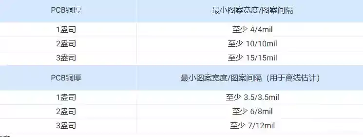
An mSAP substrate is used when conventional PCB etching cannot provide enough routing density around fine-pitch components. Instead of removing most of a relatively thick copper foil, the modified semi-additive process begins with a very thin copper layer and selectively adds copper where conductors are required.
This change in manufacturing logic allows an mSAP substrate to support finer traces, narrower spaces and more compact microvia structures. However, fine lines are not produced by imaging accuracy alone. Copper thickness, plating uniformity, seed-layer removal, material stability and contamination control must operate within the same process window.
Why Conventional Subtractive Etching Reaches a Limit
Traditional PCB fabrication begins with copper-clad material. Photoresist protects the required conductor pattern, while the surrounding copper is removed by chemical etching.
The etchant does not move only downward. It also attacks the sides of the conductor beneath the resist, producing lateral etching. As the intended trace becomes narrower, this side etching represents a larger percentage of the conductor width.
A manufacturer can compensate by making the initial image wider, but compensation becomes difficult when both the line and the adjacent space are small. Excessive compensation reduces spacing, while insufficient compensation produces narrow conductor tops or inconsistent impedance.
This is why an mSAP substrate becomes relevant for substrate-like PCBs, compact mobile products, advanced computing modules and other assemblies that require more routing channels within a limited area.
What Makes the Modified Semi Additive Process Different
The difference becomes clearer when conventional subtractive processing mSAP and SAP are compared at each circuit formation stage.
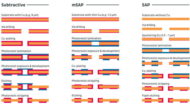
Unlike conventional subtractive processing, mSAP begins with a much thinner copper layer and builds the required conductors through pattern plating. The remaining base copper can then be removed with less lateral etching. SAP begins without copper foil and adds a separate seed layer, enabling still finer structures but requiring a more specialized process.
The modified semi-additive process starts with a thin base copper layer rather than the thicker copper normally used for subtractive fabrication. Laser-drilled microvias are cleaned and metallized, after which dry-film photoresist is applied and patterned.
Copper is then electroplated into the openings in the resist. The process builds the traces and fills or plates the microvias only in the required locations. After the target copper thickness has been reached, the resist is stripped.
A brief differential or flash-etching stage removes the exposed base copper remaining between the plated conductors. Because this unwanted copper layer is thin, considerably less etching is required than in a conventional subtractive process.
As a result, the conductor experiences less lateral erosion. The traces formed on an mSAP substrate can therefore have straighter sidewalls and more consistent widths than traces etched from thicker copper foil. IPC technical material describes this use of thin base copper followed by pattern plating and seed-layer removal as the central difference between conventional and mSAP production.
The process sequence can be summarized as:
Thin the base copper → Drill and metallize microvias → Apply photoresist → Image the circuit → Electroplate traces and vias → Strip the resist → Remove the exposed base copper
Although the sequence appears straightforward, each stage changes the operating window of the next. Uneven base copper increases final etching variation. Poor resist adhesion allows plating solution to enter unintended areas, while nonuniform current distribution changes the height and width of plated conductors.
For this reason, an mSAP substrate should be treated as a complete manufacturing system rather than a normal PCB with a more accurate imaging step.
Copper Plating Controls the Final Conductor Geometry
Laser direct imaging defines where copper can be deposited, but electroplating determines how the conductor grows. Current density, solution circulation, panel loading and feature distribution all influence plating thickness.
Dense conductor areas and isolated features may plate at different rates. If this variation is not controlled, some traces can exceed their target height while others remain too thin. Uneven plating can also reduce the amount of copper available inside microvias.
The fine conductors on an mSAP substrate require a plating process that maintains uniform thickness across the panel and inside small vias. Additive chemistry must support copper deposition without creating excessive nodules, surface roughness or voids.
Recent research on mSAP electroplating identifies plating uniformity, via filling and defects such as voids or V-shaped etching damage as significant reliability concerns. These problems matter because a conductor can pass an initial continuity test while still containing a weak section that becomes vulnerable during thermal cycling.
Seed Layer Removal Determines the Final Spacing
After plating and resist stripping, a thin copper layer still connects the conductors. It must be removed completely to create electrical isolation.
Insufficient etching can leave copper residue between adjacent traces, producing leakage or short circuits. Excessive etching removes copper from the sides and top of the intended conductors, reducing their cross-sectional area.
This is one of the most important control points in an mSAP substrate. The objective is not simply to remove visible copper, but to clear the seed layer consistently without damaging the plated circuit.
The condition of the copper surface also matters. Residues from activation, imaging or stripping processes can change the local etching rate. Cleanliness must therefore be controlled before the panel reaches the final copper-removal stage.
Material Stability Becomes More Important as Features Shrink
Fine conductor geometry is useful only when different layers remain aligned. During lamination, chemical treatment and thermal processing, the dielectric material expands and contracts. Small dimensional changes can shift pads relative to laser-drilled microvias.
An mSAP substrate consequently requires materials with suitable dimensional stability, mechanical strength and thermal behavior. The dielectric surface must also provide adequate copper adhesion without becoming excessively rough.
A rough interface can improve mechanical anchoring, but it may increase conductor loss at high frequencies. Research presented through IPC notes the need to balance a smooth dielectric interface for signal performance with sufficient copper adhesion for manufacturing reliability.
Microvias Must Be Evaluated With the Fine Lines
mSAP technology is frequently combined with laser-drilled blind microvias because narrow traces alone cannot solve routing congestion between layers. The microvia connects the fine outer pattern to the internal routing structure.
On an mSAP substrate, incomplete desmear can reduce copper adhesion inside the via, while poor metallization can create voids or weak interfaces. Uneven via filling may also leave a depression that affects later imaging and lamination.
The trace and microvia should therefore be qualified as one interconnect structure. Cross-section inspection needs to evaluate conductor dimensions, via filling, interface condition and copper thickness rather than checking only the visible surface pattern.
Inspection Must Measure More Than Line Width
Automated optical inspection can detect opens, shorts and pattern deviations, but it cannot fully evaluate copper thickness or internal microvia quality. Cross-section analysis, resistance testing and reliability testing are required to confirm that the process has produced a mechanically stable interconnect.
For an mSAP substrate entering production, useful inspection data includes the conductor width at different heights, copper thickness, spacing after seed-layer removal, microvia fill condition and registration between layers.
Statistical measurements are more valuable than a single approved cross-section. Fine-line yield depends on process distribution across the complete panel, especially near areas where plating current or chemical flow may differ.
When an mSAP Substrate Is the Right Choice
mSAP should not automatically replace conventional PCB fabrication. Standard subtractive processing remains more economical when the required line width, spacing and component pitch fit comfortably within established HDI capability.
The higher process cost of an mSAP substrate is justified when fine-pitch packages create routing congestion, when conventional designs require too many build-up layers or when reducing PCB size has significant product value. Hybrid stack-ups may also be used, placing mSAP features only on the layers that need the highest routing density.
Before production, the buyer should confirm the manufacturer’s demonstrated line-and-space capability, microvia structure, dielectric options, plating-uniformity controls and inspection plan. A quoted minimum feature size is not sufficient unless it is supported by achievable production tolerances and yield data.
For projects requiring fine-line HDI or substrate-like PCB construction, iPCB can review the stack-up, conductor geometry, microvia arrangement and inspection requirements before selecting an appropriate manufacturing process.
Fine Lines Depend on the Entire Process
The main advantage of an mSAP substrate is its ability to build copper conductors with less lateral etching than conventional subtractive fabrication. That advantage makes narrower traces, tighter spacing and higher routing density possible.
Reliable production still depends on more than the word mSAP appearing on a fabrication drawing. Thin base-copper control, resist imaging, uniform electroplating, complete seed-layer removal, stable dielectric materials and suitable inspection must function as one connected process. When these conditions are controlled, an mSAP substrate provides a practical route from conventional HDI boards toward substrate-level interconnection density.