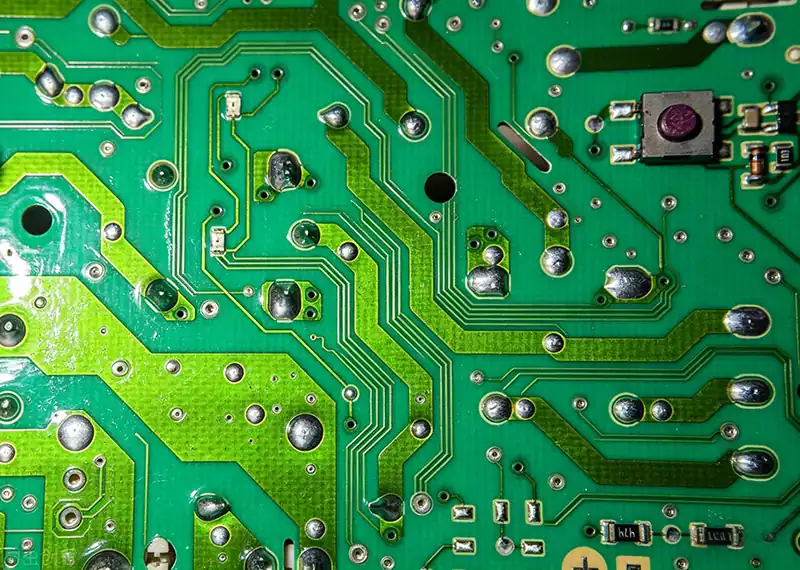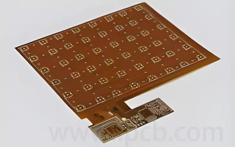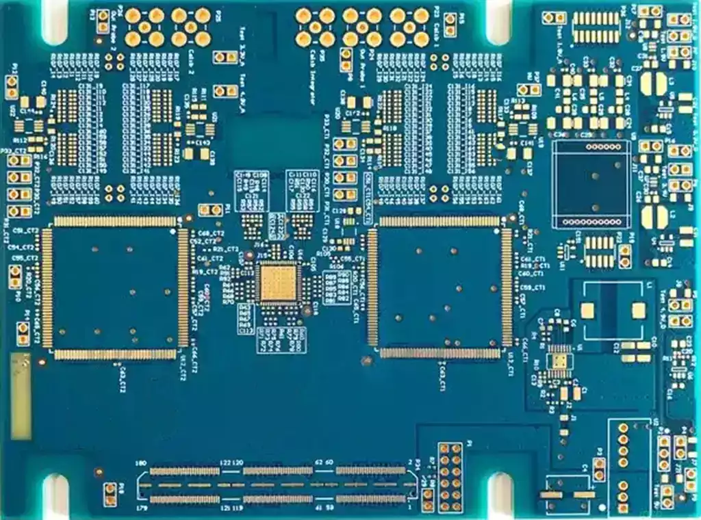
Bare board testing verifies the electrical connectivity of an unpopulated printed circuit board before components are installed. Its primary purpose is to confirm that every conductive network follows the intended design and that electrically separate networks remain isolated. Without effective bare board testing, a PCB can pass visual inspection and still contain an open circuit, an unintended short or a defective plated connection. Once components have been assembled, identifying whether the failure originated in the bare PCB, soldering process or component itself becomes considerably more difficult.
Electrical Defects Can Remain Invisible
PCB fabrication involves imaging, etching, drilling, lamination, copper plating and surface finishing. A small deviation during any of these operations may alter the finished electrical network. An incomplete conductor can create an open circuit. Residual copper between adjacent traces may produce a short circuit, while inadequate plating inside a via can form an intermittent connection. These defects are particularly important on multilayer, fine-pitch and HDI boards because many connections cannot be inspected directly.
Bare board testing compares the physical PCB against electrical test data derived from the design files. Continuity measurements confirm that points belonging to the same net are connected. Isolation measurements check that independent nets have not become electrically connected.
IPC-9252 describes electrical testing of unpopulated printed boards as a method of verifying that conductive networks are interconnected according to design requirements. It also notes that electrical testing does not replace inspections for dimensional accuracy, solder mask, conductor geometry or hole quality.
The Two Defects That Matter Most
An open circuit means a required conductive path has been interrupted. The break may occur in a trace, annular ring, via barrel or internal-layer connection. Complete opens are usually straightforward to detect, but marginal connections can become more difficult because they may conduct during testing and fail after thermal or mechanical stress.
A short circuit is an unintended connection between separate electrical networks. It may result from overplating, incomplete etching, foreign copper or internal-layer misregistration. A short between power and ground can prevent the assembly from operating, while a high-resistance bridge between signal nets may create intermittent behaviour.
For these reasons, bare board testing must check both continuity within each required network and isolation between networks that should remain separate. Testing only one condition leaves a significant portion of PCB electrical risk uncontrolled.
Why Visual Inspection Is Not Enough
Automatic optical inspection can identify conductor-width deviations, exposed copper and other visible surface defects. It cannot reliably verify every internal connection in a multilayer PCB.
A via may appear acceptable at its external pad while containing a poorly plated barrel. Internal copper features are enclosed after lamination, and a very small bridge may be hidden below solder mask. Bare board testing provides electrical evidence for these features rather than relying on their visible appearance.
Electrical results should still be combined with optical inspection, dimensional measurement and, where required, microsection analysis. Each method evaluates a different aspect of PCB quality.
Fixture Testing for Stable Production Volumes
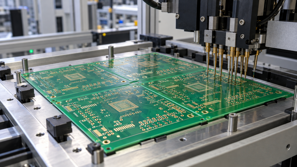
A dedicated test fixture uses a bed of probes aligned with test points on the PCB. When the board is placed in the fixture, many electrical connections can be evaluated in a short test cycle.
This makes fixture-based bare board testing suitable for repeated medium- and high-volume production. The initial fixture requires engineering time and tooling cost, but its fast cycle time can reduce the testing cost per board across a large order.
Fixture accuracy depends on correct probe access, board registration and mechanical support. Fine-pitch designs may require specialised probe technology, while thin boards need adequate support to prevent bending during contact.
A fixture must also match the correct PCB revision. If the layout changes but the test data or fixture does not, valid boards may be rejected or incorrect connectivity may remain undetected. Revision control is therefore part of the bare board testing process rather than an administrative detail.
Flying Probe Testing for Prototypes and Small Batches
Flying probe equipment moves independently controlled probes between accessible PCB locations. Because it does not require a dedicated bed-of-nails fixture, the test program can be generated directly from PCB design data.
This gives flying probe bare board testing a clear advantage for prototypes, engineering revisions and low-volume orders. Setup costs remain relatively low, and modified PCB data can be introduced without manufacturing a completely new fixture.
The trade-off is test speed. Probes must move between individual locations, so cycle time generally increases with net count, board density and required coverage. For a few prototypes this may be insignificant, but it can become a production constraint when thousands of identical boards are required.
Flying probe access must still be considered during design. Solder-mask openings, very small pads, tall board features and test points located close to the edge can affect probe contact. Electrical testability should consequently be reviewed before the manufacturing data is released.
Choosing the Appropriate Test Method
The choice between flying probe and fixture testing is primarily controlled by production volume, PCB revision stability, layout density and delivery requirements.
A new design that may change after functional evaluation normally benefits from flying probe testing. A stable design ordered repeatedly in larger quantities can justify the cost of a dedicated fixture. Some manufacturers use flying probes during prototype validation and change to fixture testing after the design enters volume production.
Neither method should be selected only from the price shown on an initial quotation. Effective bare board testing must provide sufficient coverage, suitable resistance limits, correct design data and traceable results. A low-cost test with incomplete access or outdated net data provides limited protection.
Test Data Must Follow the Correct Revision
Electrical testing is only as reliable as its reference data. The manufacturer may derive the test program from Gerber data, IPC-356 netlist data or another approved manufacturing dataset.
Using an independent netlist is valuable because it allows the finished connectivity to be checked against information that is not reconstructed only from the PCB image files. File names, revision identifiers and panel transformations must remain controlled throughout production.
Bare board testing records can include the tested part number, revision, panel or lot identification, test method and pass or fail status. For higher-reliability products, retaining this information helps connect a finished assembly failure to its original PCB manufacturing batch.
A Passed Electrical Test Does Not Prove Everything
A board that passes bare board testing has met the defined electrical continuity and isolation conditions at the time of testing. This result does not automatically prove that hole dimensions, solder-mask registration, surface finish, cleanliness or impedance are acceptable.
It may also fail to reveal a marginal structure that changes after reflow unless the specified test limits and additional reliability controls address that risk. Electrical testing should therefore be treated as one part of the PCB quality plan.
The required checks depend on the product. A simple two-layer control PCB and a high-density multilayer communication board do not carry the same structural or reliability risks.
When Bare Board Testing Should Be Specified
Electrical testing is valuable whenever a PCB defect would waste expensive components, create difficult troubleshooting or compromise field reliability. It becomes especially important for multilayer boards, dense BGA layouts, HDI structures, high-value assemblies and products that are difficult to repair after installation.
Purchase documentation should define whether every board requires testing, which data controls the test program and whether test records or certificates must accompany the shipment. These details prevent different suppliers from interpreting the requirement differently.
At iPCB, bare board testing can be integrated with fabrication inspection and manufacturing-data review before boards are released for assembly. Matching the test program to the approved PCB revision helps prevent fabrication defects from being carried into component placement and reflow.
Preventing Assembly Cost From Being Added to a Defective PCB
The cost of detecting an open or short is lowest before the PCB receives components. After assembly, the same defect may consume solder paste, electronic parts, machine time, inspection capacity and troubleshooting labour. If it remains intermittent, it may not appear until final system testing or field operation.
Bare board testing creates an electrical quality gate between PCB fabrication and PCBA production. It does not replace dimensional, structural or visual inspection, but it prevents boards with incorrect connectivity from receiving additional manufacturing value. When test coverage, revision control and production volume are considered together, bare board testing becomes a practical method of protecting assembly yield rather than merely an optional inspection step.