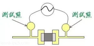
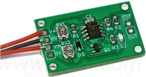
Why are test points needed on PCB circuit boards?
Test points are an important design element in printed circuit boards and can be used as locations to probe signals or apply test stimuli during development, verification, debugging, field service

Key Technologies of USB Hub PCB Board
In today’s digital age, USB hub circuit boards have become a key component for connecting multiple devices. With the continuous advancement of technology, users’ growing demand for data transmission speed,
Types and selection of circuit board etchant
Circuit board etchant is a chemical reagent essential to the production process of printed circuit boards, mainly used to remove the copper foil portion of the printed circuit board that
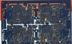
Power supply pcb slot hole design
In the rapid development of electronic technology, power supply pcb as one of the core components of electronic equipment, its design quality is directly related to the stability and safety
Functions and Classification of pcb button
A pcb button is a pushbutton or switch mounted on a circuit board that receives input signals from the user and converts them into electronic signals to control the operation
Plated half hole process flow and difficulties
Plated half holes are similar to plated through-holes, but occupy only half of the vertical space. This design makes them structurally more compact while maintaining good electrical and mechanical connectivity.
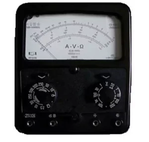
How to test a switch using a multimeter
In the daily maintenance and troubleshooting of electronic equipment and electrical systems, the reliability of the switch, as a key component of the circuit control, directly affects the safety and
Mini Breadboard Usage and Function
Mini Breadboard that is, ‘integrated circuit experiment board’, is a plug-in board, this ‘board’ has a number of small ‘socket (hole)’. When conducting circuit experiments, you can insert the pins
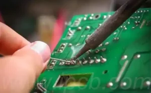
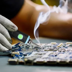
How do you solder wires to a circuit board
In the world of electronics fabrication and repair, the skill of ‘how do you solder wires to a circuit board’ is critical. Whether you are experimenting with simple circuits or
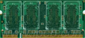
PCB Circuit Board Layer Structure
PCB circuit board infrastructure is equivalent to a building’s foundation and framework, which consists of four main layers: top layer (Top Layer), bottom layer (Bottom Layer), inner layer (Inner Layer)
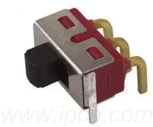
Printed circuit board switches
What is printed circuit board switches?Printed circuit board switches is an electronic component used to control circuit on/off, function selection, etc. It is one of the more common components on
PCB Etching Process Essentials
In the PCB circuit board printing process, the transformation of a bare board into a finished product with clear circuit graphics requires a series of sophisticated physical and chemical reactions,
The central role of Photoresist pcb boards
Photoresist pcb boards are printed circuit boards manufactured using photoresist technology.The photoresist used in Photoresist pcb boards is a light-sensitive material that is usually applied to the surface of the
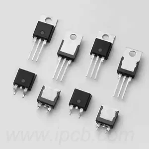
Impact and selection of active high frequency components
Active components are key components in electronic circuits that can be powered from an external source to perform functions such as signal amplification, conversion, and generation. Active high frequency components
What is a protoboard?
What is a protoboard?A protoboard, also known as a ProtoType board, is essentially an early sample of a product that is designed to test a design idea and see if
Crazing pcb causes and prevention
Crazing pcb is the phenomenon of cracks or breaks in a circuit board, which can lead to impaired functionality or even complete failure of the board. The causes of crazing
How to choose the right pcba process
Selecting the right PCBA process is a strategic decision that can have a decisive impact on product quality, productivity and cost-effectiveness. In the face of a wide range of process
Impact of the HASL process on PCB Board
The tin spraying process, also known as hasl, is a long-established technology for PCB (Printed Circuit Board) surface treatment. The process starts by immersing the PCB in molten solder, which
How to Make a Breadboard Permanent
When a circuit design has been tested many times and confirmed to be feasible, it is necessary to consider how to make the breadboard permanent to ensure the stability and
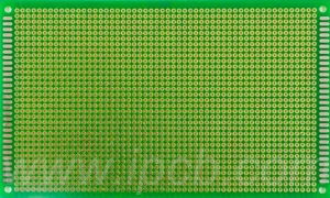
Application of board electronics with holes
A board electronics with holes is a substrate used for the layout of electronic components and its function is to connect electronic components. It is a design element on a
Selection and Importance of circuit board enclosure
A circuit board enclosure is a material specifically designed to protect circuit boards from damage or contamination. It also enhances the mechanical strength and thermal resistance of the circuit board,
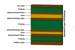
6 layer pcb stackup design
A 6 layer pcb stackup structure is a design in which six layers of conductive and non-conductive materials are stacked together during the circuit board manufacturing process to achieve complex
Selection of 96% and 99% alumina ceramic substrate
Alumina ceramic substrates consist mainly of a white amorphous powder commonly known as aluminium oxide, or simply Al2O3. It has a density of between 3.9 and 4.0 g/cm3, a melting
IC Board Component Layout Optimisation
As a core component, the design and layout of an integrated circuit board (IC board) has a direct impact on the performance, reliability, and productivity of the device.The layout of