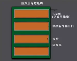
Criticality of PCB soldermask opening
Soldermask opening is a crucial part of the PCB (Printed Circuit Board) design and manufacturing process. The main purpose of the soldermask is to prevent accidental flow of solder during
flux paste vs solder paste
I believe that many people will confuse flux paste with solder paste. In fact, they are different. Solder paste is tin paste. Its main component is a paste composed of
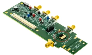
Design and Application of HF Bandpass Filter PCB
With the rapid development of communication technology, high-frequency bandpass filters (HF Bandpass Filter) are increasingly used in wireless communication, radar, audio processing and other fields.As an electronic component that allows
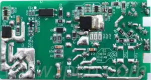
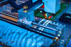
Wave soldering process optimisation
As an integral part of the electronics manufacturing industry, wave soldering has a direct impact on the performance and reliability of electronic products in terms of soldering quality. Optimising the
Difference between wave soldering and reflow soldering
Wave soldering, also known as surge wave soldering, is a method of forming wave-like peaks through molten solder, so that the pads and component pins on the circuit board can
Why preheat before PCBA soldering
In the pcba assembly process, welding is a key step in connecting various components together. In order to ensure the quality and effect of welding, pcba pre-soldering preheating becomes a
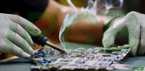
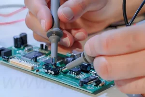
How to solder wire to pcb board
Soldering wire precisely and securely to a pcb board is a fundamental and critical skill in the assembly and repair of electronic equipment. Whether you’re a DIY enthusiast or a
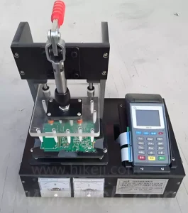
Circuit Board Repair Tools
In circuit board repair, a DC regulated power supply is often needed to supply power to the circuit board in order to test the working condition of the circuit. There
Printed Circuit Board Repair Tips
Printed circuit board repair, as an important part of the maintenance of electronic equipment, is vital to ensure the proper functioning of the equipment. It is important to understand the
Applications and Challenges of BGA PCB Board
As electronic devices continue to develop towards miniaturization, high performance and low power consumption, BGA (Ball Grid Array) circuit board technology has gradually become an important part of modern electronic
Why double sided ceramic pcb boards
Double sided ceramic pcb board, also known as double sided ceramic circuit board, is commonly found in many electronic products that are used on a daily basis. While single-sided ceramic
PCB Board Graphics Transfer and Plating Technology
The graphics transfer step in the double sided PCB board manufacturing process is a critical part of the process to accurately reproduce the designed circuit pattern onto the copper board.
DCC adapter pcb board
DCC adapter pcb board is an important piece of equipment designed for model railway enthusiasts and professional engineers to enable conversion between digital control systems and analogue signals.These pcb boards
The Importance of Hard Disk Circuit Board
The hard disk circuit board is an important part of the hard disk and one of the core components for data storage and reading and writing. It connects the mechanical
FR-4 fixture is the cornerstone of electronic testing
FR-4 fixture, its core material is FR-4 glass fibre board, which is a composite material with epoxy resin as the binder and electronic grade glass fibre cloth as the reinforcing
welding paste
Welding paste is a homogeneous mixture, a paste with a certain viscosity and good thixotropy, which is a mixture of alloy solder powder, paste flux and some additives. It is
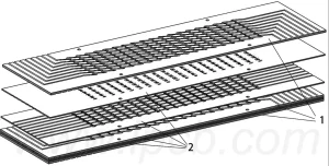
Printed Circuit Board Heat Exchanger
The Printed Circuit Board Heat Exchanger (PCB-HEX) is a highly efficient compact heat exchanger manufactured using printed circuit board technology, which is characterised by the fact that the metal wires
How much does a pcb board cost
While it is true that there are some generally applicable basic processes in the PCB board industry, it is even more critical to carefully select and determine the appropriate production
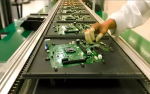
PCBA processing requirements for PCB boards
In the field of electronics manufacturing, PCBA chip processing constitutes a core link in the product manufacturing process, and plays a decisive role in the performance, stability and durability of
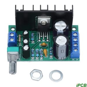
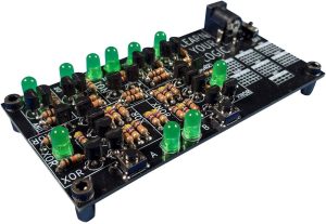
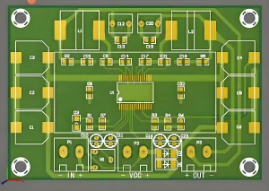
amplifier board
What is an amplifier board? As the name implies, an amplifier PCB is a circuit that can “amplify” a specific input signal. Amplification means obtaining an enhanced signal gain using
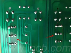
Double Sided PCB Soldering Tips
PCB soldering precautions1.EDA365 electronic community suggests that the first task after obtaining the PCB bare board is to carry out visual inspection to confirm that there are no short circuits,
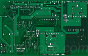
Double sided pcb board manufacturing process challenges
The production process for double sided pcb board consists of several stages, each of which may face a number of technical challenges.The following are some of the major challenges: Design
How to Wire PCB mono input jack
In the design of modern electronic products, audio input and output are very important, especially in the design of audio equipment. As part of the audio equipment, the mono input
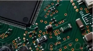
PCBA SMD preparation and processing considerations
PCBA chip processing is one of the core links in the manufacturing process of electronic products, which includes a number of stages from circuit design to product moulding. Each stage