A circular PCB board, also known as a round printed circuit board, is a printed circuit board whose outline is circular or nearly circular rather than the conventional rectangular shape. In terms of electrical performance, a circular PCB board operates on the same basic principles as other PCBs: copper traces connect electronic components, while vias provide electrical connections between different layers. The primary difference lies in the board’s mechanical form factor, which affects component placement, routing, panelization, assembly, and enclosure integration.
Depending on the electrical complexity of the application, a circular PCB board can be manufactured as a single-sided, double-sided, or multilayer PCB. It can also be fabricated from various PCB materials, including FR-4, aluminum-based materials, ceramic substrates, flexible materials, and other specialty laminates. The circular shape does not change the fundamental principles of PCB construction. Instead, it changes how the circuitry must be laid out within the available space.
A circular PCB board may also include a center hole, mounting holes, slots, edge notches, connector cutouts, or large internal cutouts. Therefore, the term does not necessarily refer to a completely solid circular disk.
Rectangular PCBs remain more common because their geometry simplifies component placement, PCB routing, panelization, assembly processes, and enclosure integration. However, circular PCB boards become more practical when the product itself has a circular or curved form factor. For example, a rectangular PCB may use space inefficiently inside a circular enclosure because its corners can occupy areas that cannot be effectively utilized.
When properly designed, a circular PCB board can conform more closely to the enclosure and allow components to be arranged around the available usable area. This is particularly useful in products where the PCB is an important part of the mechanical structure rather than simply a flat electrical carrier.
Why Use a circular PCB board?
The primary reason for using a circular PCB board is generally mechanical integration rather than an inherent electrical advantage. When a product has a circular or curved enclosure, a circular circuit board can make better use of the available internal space and eliminate the unused corners that would occur with a rectangular PCB. This can help engineers develop smaller and more highly integrated products.
Applications such as wearable devices, compact sensors, LED modules, circular control interfaces, and other space-constrained products can benefit from this approach.
A circular form factor can also simplify integration with rotational or radial structures. Components can be distributed around a central axis, while connectors, sensors, LEDs, and other functional components can be positioned according to the mechanical requirements of the product. This makes circular PCB boards particularly suitable for devices in which the PCB must conform to a circular enclosure or support a radial component arrangement.
However, a circular shape should not automatically be considered electrically superior to a rectangular PCB. Claims that simply eliminating sharp corners always improves signal integrity or significantly reduces electromagnetic interference (EMI) are too broad.
Electrical performance is primarily determined by factors such as trace geometry, controlled impedance, return paths, stackup design, grounding, component placement, and operating frequency. A circular outline can support specific routing strategies, but the board shape itself does not guarantee better high-frequency performance.
How Are Circular PCB boards Manufactured?
The manufacturing process for a circular PCB board is fundamentally similar to that of a rectangular PCB. Manufacturers can use standard PCB fabrication processes to form the required copper layers, laminate multilayer structures, drill holes, plate vias, apply solder mask, perform surface finishing, and conduct electrical testing.
The primary additional consideration is the board outline. The circular profile must be accurately milled or formed according to the mechanical drawings and manufacturing data.
During production, multiple circular PCB boards are typically arranged together on a larger production panel. Panelization can be more challenging than with rectangular PCBs because circular boards leave unused spaces between adjacent units. This affects material utilization and may increase manufacturing costs.
Therefore, panelization must balance the number of boards per panel, board orientation, tooling requirements, routing paths, and assembly requirements. In general, the panel utilization rate of non-rectangular PCBs is often lower than that of rectangular PCBs, so panelization should be considered before the design is finalized.
The final board outline can be produced using CNC routing, profile milling, laser cutting, or other suitable PCB contouring processes. The appropriate method depends on the board material, thickness, dimensional tolerances, production volume, and required edge quality.
If the circular PCB board will be installed in a high-precision mechanical enclosure, particular attention may be required for finished board diameter, mounting-hole locations, and mechanical tolerances.
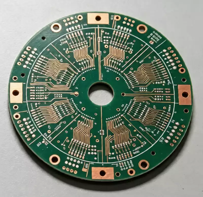
Circular PCB board Design Considerations
One of the biggest design challenges is the curved board edge. On a rectangular PCB, engineers can easily use straight edges as references for component placement and routing. On a circular PCB board, the available area continuously changes toward the perimeter.
Components with rectangular packages may not be efficiently placed near the curved edge, potentially leaving unused space between the component body and the board outline. Therefore, the theoretical area of a circular PCB board does not necessarily represent the actual area available for component placement.
Component placement should therefore be planned around the mechanical and functional requirements of the PCB. Larger components are generally better suited to the central area, while smaller components can be positioned closer to the perimeter when sufficient clearance is available.
Connectors, switches, LEDs, sensors, mounting holes, and other mechanically constrained components should be positioned according to the enclosure and assembly requirements rather than simply filling the board outward from the center.
The board outline should also be precisely defined in the PCB design data. For a custom circular PCB board, specifying only the nominal diameter is usually insufficient. The mechanical design may also need to define the center position, mounting-hole locations, hole diameters, slots, notches, connector cutouts, board thickness, component height restrictions, and applicable mechanical tolerances.
For complex assemblies, the PCB should be checked together with the enclosure, connectors, heat sinks, lenses, and other mechanical components before manufacturing.
Routing Considerations
Routing may also require a different approach. Instead of treating the PCB as a conventional rectangular grid, engineers may need to route traces according to the circular geometry and available radial space.
Regardless of the board shape, high-speed signals still require controlled impedance, appropriate reference planes, and properly designed return paths. Power and ground distribution should also be considered at an early stage because the curved perimeter can make consistent component placement and routing density more difficult.
For RF and high-speed designs, the designer should pay particular attention to trace width, dielectric properties, reference-plane continuity, return current paths, via transitions, and impedance control rather than assuming that the circular outline itself provides an electrical benefit.
Circular PCB board vs. Rectangular PCB
A circular PCB board is not inherently better than a rectangular PCB. Each form factor addresses different design requirements.
Rectangular PCBs are generally easier to manufacture, panelize, assemble, and package efficiently. They also provide a more predictable layout area because most electronic components use rectangular package geometries.
When the product enclosure or mechanical structure is circular, however, a circular PCB board can become more attractive. In such applications, a rectangular board may create unused corner areas and reduce internal assembly efficiency. A circular design can conform more closely to the available mechanical space and provide a more integrated product structure.
The trade-off is that routing and panelization can be more challenging. The curved perimeter reduces the practical placement area near the edge, while multiple circular boards cannot generally be nested as efficiently as rectangular boards.
These factors can increase material waste and manufacturing complexity. Therefore, the decision should be based on the complete product design rather than the PCB shape alone.
Are Circular PCB boards More Expensive?
A circular PCB board is not necessarily more expensive simply because it has a circular outline. However, the shape can introduce additional manufacturing considerations.
The most significant factor is often panel utilization. Rectangular PCBs can usually be nested closely together with relatively little unused material, whereas circular PCB boards leave gaps between adjacent boards. This reduces the number of individual boards that can fit on a production panel and can increase material consumption.
The routing and profiling process can also affect manufacturing time. However, modern PCB manufacturing equipment can produce circular and other non-rectangular board outlines without fundamentally changing the overall PCB fabrication process.
Actual cost depends on factors such as board dimensions, layer count, substrate material, copper thickness, dimensional tolerances, surface finish, order quantity, assembly requirements, and panelization strategy, rather than the circular shape alone.
A circular PCB board is a printed circuit board designed with a circular or curved outline to meet specific electrical, mechanical, or product-design requirements. Its fundamental construction and electrical operating principles are the same as those of conventional PCBs. However, its form factor changes how engineers approach component placement, PCB routing, mechanical integration, panelization, manufacturing, and assembly.
For products with circular enclosures, radial component arrangements, or strict space constraints, a circular PCB board can provide better mechanical integration and more efficient use of the available space. However, designers should evaluate layout efficiency, controlled impedance, manufacturability, panel utilization, mechanical tolerances, and overall cost before selecting a circular PCB board over a conventional rectangular design.