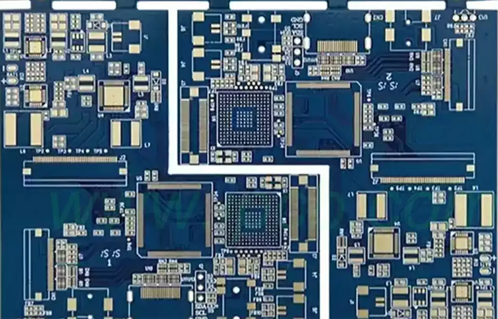
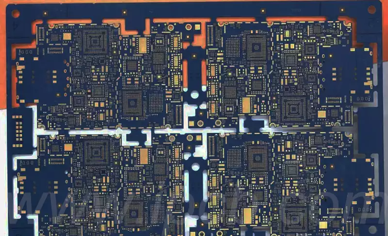
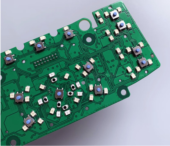
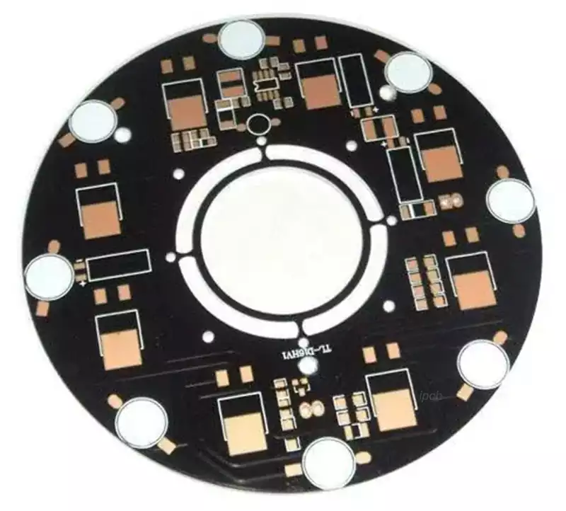
A microvia PCB uses very small blind or buried interconnections to connect conductive layers within a high-density circuit board. Microvias are commonly formed with laser drilling and are widely associated with HDI PCB technology, where conventional through-holes may consume too much routing space. By reducing the size of the interconnection structure, microvias allow designers to place more connections within a limited board area.
Microvias are different from conventional through-hole vias because they generally connect only selected layers rather than passing through the entire PCB. Their small geometry also changes the way the board is designed and manufactured. Layer structure, dielectric thickness, laser parameters, copper plating, via arrangement, and reliability requirements all need to be considered together.
For compact electronic products, this approach can provide additional routing density while allowing the overall PCB size to remain relatively small. However, a microvia PCB requires tighter process control than a conventional multilayer board because the small features leave less manufacturing margin.
A microvia is a small-diameter interconnection that typically connects an outer layer to an adjacent inner layer or connects selected layers within an HDI structure. IPC defines a microvia as a blind structure with a target land diameter of 0.15 mm or less when measured at the land on the target layer. The actual design dimensions can vary according to the manufacturing process and applicable design requirements.
Laser drilling is commonly used to form microvias because the required hole dimensions can be much smaller than those normally produced by mechanical drilling. After the dielectric material is processed, the resulting hole is metallized so that electrical continuity can be established between the connected copper layers.
A conventional through-hole via extends through multiple PCB layers, while a microvia generally connects only a limited number of layers. This difference is important when planning an HDI stack-up. Instead of routing every signal through a large through-hole structure, designers can use microvias to create shorter vertical connections between specific layers.
Microvias can also be arranged in different structures. Depending on the board design and fabrication process, they may be used as staggered microvias or stacked microvias. Staggered structures place microvias at different locations on adjacent layers, while stacked structures place one microvia above another to establish a vertical interconnection through several layers.
These structures provide greater routing flexibility, but they also introduce additional manufacturing considerations. The selected structure needs to be compatible with dielectric thickness, laser processing, copper plating, registration accuracy, and reliability requirements.
Microvia PCB Design Considerations
The design of a microvia PCB starts with the layer stack-up. Designers need to know which layers will be connected, where the microvias will be placed, and how much routing space remains around the via structures. Because microvias are small, they can help free routing space that would otherwise be occupied by larger conventional vias.
Via-in-pad is one example of how microvias can be used in high-density layouts. A microvia can be positioned within a component pad to provide a short connection to another layer. This can be useful for fine-pitch packages where conventional via placement would interfere with adjacent pads or traces. However, via-in-pad construction requires an appropriate fabrication process because the via opening may need to be filled and processed so that it does not create problems during component assembly.
The relationship between the microvia and its target land is also important. Land size, capture pad dimensions, drill geometry, dielectric thickness, and spacing all affect the manufacturability of the structure. The aspect ratio of the microvia needs to remain within the capability of the selected fabrication process.
Microvia placement should also take electrical requirements into account. High-speed signals can be affected by discontinuities in the interconnection path, so designers may need to consider signal transitions, reference planes, return-current paths, and via arrangements. For power distribution, the number and arrangement of interconnections may need to be evaluated according to current requirements rather than simply the available routing space.
The design should therefore be developed around the complete HDI stack-up instead of treating each microvia as an isolated feature. The PCB fabricator’s process capability should be considered before the dimensions are finalized, particularly when the design uses stacked microvias, fine-pitch components, or multiple sequential buildup layers.
Microvia PCB Manufacturing Process
Microvia PCB manufacturing commonly uses sequential buildup processes. A dielectric layer and copper are added to the existing board structure, laser drilling is used to create the required microvia openings, and the holes are metallized to establish electrical connections. Additional buildup cycles may be performed when the design requires connections across several buildup layers.
Laser drilling is a key part of the process because the beam must create the intended microvia geometry without damaging the surrounding material or the target copper layer. Laser parameters depend on the dielectric system, copper thickness, hole dimensions, and fabrication process. After drilling, cleaning and desmear processes may be required before copper plating.
Copper plating is particularly important because the microvia has a small internal surface area and needs a reliable conductive connection. The plating process must provide sufficient copper coverage through the microvia and at its connection points. For stacked structures, the reliability of each successive connection becomes important because manufacturing variation can accumulate through the buildup structure.
Registration accuracy is another critical manufacturing factor. The laser-drilled microvia must align correctly with the target land on the underlying layer. As the number of buildup layers increases, layer-to-layer registration becomes increasingly important.
After fabrication, inspection and electrical testing can be used to verify the finished board. Depending on the design, inspection may include dimensional checks, automated optical inspection, electrical testing, and other process-specific evaluations. Microvia reliability may also be evaluated through appropriate qualification and reliability testing when required by the product.
Microvia PCB Reliability and Applications
The reliability of a microvia PCB depends on the complete material and manufacturing structure rather than simply the diameter of the hole. Thermal cycling, copper plating quality, dielectric properties, layer registration, via geometry, and the arrangement of stacked or staggered structures can all affect long-term performance.
Thermal expansion is particularly relevant because the PCB materials and copper interconnections respond differently to temperature changes. Repeated thermal cycling can place mechanical stress on the microvia structure. This makes material selection, plating quality, and the geometry of the buildup layers important considerations during design and process development.
Applications that require high routing density can benefit from microvia technology. These include compact computing hardware, mobile electronics, high-density communication equipment, advanced control systems, and other products where component pitch and board area place significant constraints on routing.
Microvias are also useful when fine-pitch packages require short connections between component pads and internal routing layers. Instead of allocating board space to larger through-hole vias, a microvia structure can provide a more localized connection and preserve additional routing channels.
A microvia PCB should therefore be designed as a complete HDI system rather than simply a conventional PCB containing smaller holes. The layer stack-up, laser drilling, copper plating, via arrangement, component footprint, electrical requirements, and reliability targets all influence the final structure. When these factors are coordinated from the beginning, microvia technology can provide the interconnection density required for compact and increasingly complex electronic designs.