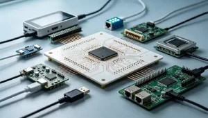
PCB Schematic and PCB Layout Design Guide
For beginners learning about PCBs, one of the most common sources of confusion is the difference between a PCB schematic and a PCB layout file. Although these two files are
Optimizing Mounting Holes PCB for Stress, EMC, and Manufacturing
In the hardware design and mechanical engineering of printed circuit boards (PCBs), mounting pcb holes, seemingly just ordinary round holes on the board, are crucial hubs connecting the electrical and
Why Ceramic Substrate Thickness Matters in Industrial Applications
In industrial applications, ceramic substrates are not limited to electronic packaging structures—they are also widely used as insulation and mechanical support components. Therefore, substrate thickness is not a parameter that
Rogers 3003 PCB Material for High Frequency and High Speed Applications
Rogers 3003 is a premium high-frequency PCB laminate developed by Rogers Corporation specifically for demanding RF, microwave, and high-speed digital applications. It has become one of the industry’s preferred substrate
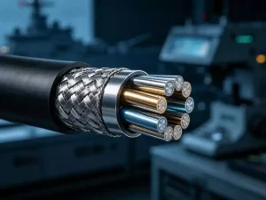
RF Cable Comparison Coaxial Twinaxial and Triaxial Cables
In the selection process of RF cables and connectors, choosing the appropriate cable type is the first and most critical step. In RF transmission systems, the three most commonly used
Optimizing Layout and Electromagnetic Performance in High Current Circuit Board
In high-power industrial power supplies, new energy vehicle powertrains, server power modules, and motor drive control systems, high current circuit boards play a crucial and unique role. Traditional circuit boards
Rogers High Frequency Laminates Performance Applications and Selection Guide
Rogers high frequency laminates are recognized as one of the industry benchmarks for high-performance materials used in RF, microwave, and millimeter-wave circuit design. Unlike conventional FR-4 laminates, Rogers materials deliver
Characteristic Impedance in High Speed PCB Design
Characteristic impedance is one of the most critical parameters in high-speed PCB design. It refers to the dynamic opposition encountered by high-frequency electrical signals as they propagate through PCB transmission
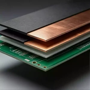
4 Layer PCB Structure and Applications
As the most widely used entry-level multilayer PCB, the 4 layer PCB provides an ideal balance between electrical performance, routing flexibility, manufacturing complexity, and production cost. Today, it is extensively
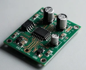
Optimizing Thermal and Grounding in pcb board amplifier
Heat Sink Design and Microscopic Electroplated Windows in PCB Board Amplifiers Power amplifiers inevitably experience significant heat loss during the conversion of DC power into AC signals. Whether it’s the
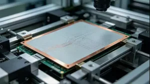
What Is an Aluminum Base PCB?
An Aluminum Base PCB is a specialized metal core printed circuit board (MCPCB) that uses an aluminum alloy substrate as its core material instead of conventional FR-4 glass fiber laminate.
High Frequency PCB vs High Speed PCB Differences Explained
High frequency PCBs and high speed PCBs are often confused because both are used in advanced electronic applications. However, they are designed for different signal types and require different materials,
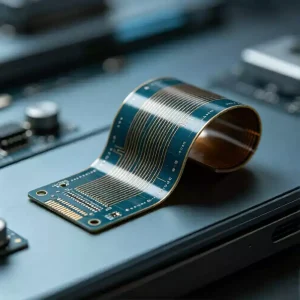
Why Flexible PCBs Are Ideal for High-Frequency Applications
Flexible PCB technology has become increasingly important as modern electronic devices continue to evolve toward higher frequencies, faster data transmission, and more compact designs. Compared with conventional rigid PCBs, flexible
Stacked Microvia Reliability in electronic pcb board
Deciphering the Electromagnetic Behavior of Electronic PCB Board Substrates The electrical performance of a printed circuit board (PCB) primarily depends on its core physical interlayer—the copper-clad laminate (CCL). Under high-frequency,
RF Front End Architecture Components and Key Technologies
The RF front end (RFFE) consists of a series of components located between the RF transceiver and the antenna. Its primary building blocks include the power amplifier (PA), RF switch,
Underfill Flow Dynamics in flip chip mounting
Unveiling the Microscopic Geometry and Interconnect Physics of Flip Chips Traditional wire bonding uses gold or copper wires to connect the electrodes on the front of the chip to the
Flip Chip Packaging Process and Copper Pillar Bump Technology
Flip Chip (FC), also known as flip chip packaging, is one of the most widely used advanced semiconductor packaging technologies in the industry. Unlike conventional wire bonding, Flip Chip technology
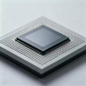
How a Hard Disk PCB Board Works
The hard disk pcb board is the core hardware that connects a hard drive to the computer’s motherboard and enables data communication between the two. It serves as the central
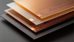
How FPCs Differ from Rigid PCBs
Flexible printed circuit boards (FPCs), also known as flexible PCBs, are an important category of printed circuit boards. However, they differ fundamentally from conventional rigid PCBs in terms of materials,
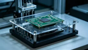
PCBA Test Fixture Functions and Applications
A PCBA test fixture is a custom-built testing tool specifically designed for assembled printed circuit board assemblies (PCBAs) in the electronics manufacturing industry. As a non-standard automated testing solution, it
Advantages and Applications of Double-Sided Ceramic PCBs
A double sided ceramic PCB, also known as a double-layer ceramic PCB, is one of the most widely used substrate types in modern electronics manufacturing. It serves as a critical
Controlling Via Impedance on bga adapter board
Decoding the Signal Integrity and Impedance of BGA Adapter Boards The core physical purpose of BGA adapter boards is to fan out the incredibly dense, unsolderable BGA pin matrix on
How Millimeter Wave PCBs Enable High Frequency Electronic Applications
Millimeter wave pcbs are specialized circuit boards designed to operate at frequencies of 24 GHz, 28 GHz, 39 GHz, 60 GHz, 77 GHz, 79 GHz, and above. They have become
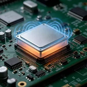
PCB Shielding for High Speed PCB and RF Circuit Design
PCB shielding is an essential design solution in high-speed electronic circuits. As PCB layouts become increasingly compact and integrated, more wireless communication modules—including GPS, Bluetooth, Wi-Fi, and 2G to 5G