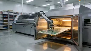
Reflow Soldering Temperature Profile for Ceramic Circuit Boards
Ceramic circuit boards, owing to their high-temperature resistance and superior thermal conductivity, have progressively become the preferred substrate for high-power electronic components. However, their inherent ceramic properties pose significant challenges
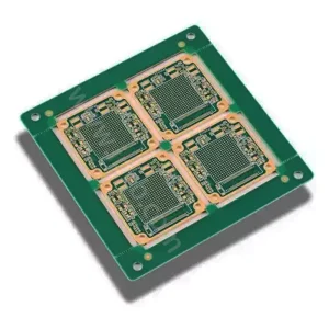
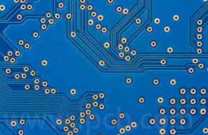
Why Prototype SMT Assembly Determines Manufacturing Success
The Core Value and Industry Positioning of Prototype SMT Assembly In today’s world of increasingly compressed electronic product development cycles, Prototype SMT Assembly is no longer just a simple step
Aluminium nitride ceramic circuit boards empower laser diode applications
Behind the faint light pulses of laser diodes lies an uncompromising demand for substrate material. From the precise detection of autonomous driving lidar to the high-speed transmission of 800G optical
Thermal Conductivity Properties and Development Trends of Ceramic Circuit Boards
When the thermal conductivity of conventional FR-4 substrates, typically below 1 W/(m·K), proves inadequate for managing the thermal loads of high-power devices, ceramic circuit boards emerge as the preferred solution.
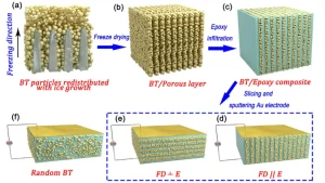
Analysis of high dielectric constant
In the wave of nanotechnology, two-dimensional materials have become a focus in the field of materials science due to their atomic scale thickness and unique physical properties. Among them, High-k
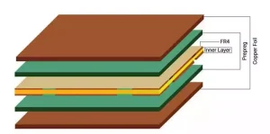
Key Considerations for PCB Laminate Design
In the field of electronic circuit design, the PCB (printed circuit board) serves as the substrate for electronic components, with its performance directly impacting the quality and reliability of the

Optical Module PCBs
As a core component in optical communications, the stability and reliability of optical modules are paramount. The optical modules pcb design not only determines their electrical performance but also plays
Ceramic circuit boards?
Ceramic circuit boards utilise ceramic as the substrate material, upon which metallic circuits are constructed and conductive vias formed. Ceramics encompass a diverse range of materials, with commonly employed types
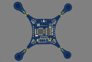
Drone PCB drives intelligent flight innovation
The Foundation of the Integration of Drones PCB Systems As highly integrated intelligent flight platforms, drone pcb have evolved from their original military reconnaissance tools to comprehensive systems widely used
PCB Circuit Board Connection Methods
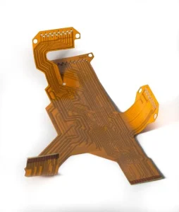
Connections between pcb circuit boards are primarily achieved through conductive connectors, wires, flexible printed circuits (FPC), board-to-board connectors, and soldering techniques. Among these, flexible printed circuits (FPC) serve as a
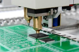
The Role and Classification of SMT Stencils in Surface Mount Technology
SMT stencils, commonly referred to as ‘templates’, are an indispensable component of the SMT (Surface Mount Technology) process; they serve as the template for printing solder paste onto the PCB
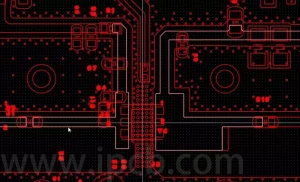
Factors Affecting PCB Trace Impedance and Calculation Methods
PCB trace impedance refers to the total resistance encountered by electrical signals during transmission across a PCB board. In layman’s terms, it represents the ‘resistance’ encountered by electrical signals as
Characteristics and Applications of Semi Flex PCB
Semi flex pcb is essentially “standard” multilayer PCBs manufactured using specific grades of FR4. The thickness of the FR4 is subject to particular tolerances, enabling thinner sections to provide the
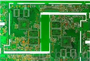
Key Considerations and Strategies for High Speed PCB Design
High speed PCB design specifically refers to systems that utilise high speed digital signals to transmit data between components. The boundary between high-speed digital design and simpler circuit boards employing
The Importance of PCB Impedance Control and Its Effects
The Impact of PCB Impedance Control on Circuit Performance and Stability. In the design of high-frequency, high-speed electronic products, the stability and reliability of circuit performance critically influence product quality.
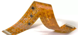
Methods for Enhancing the Reliability of Flexible PCB
Driven by innovation in consumer electronics, medical devices, aerospace, and other fields, flexible pcb (FPC) have become core components for achieving three-dimensional structural integration and dynamic functionality in devices. However,

Rapid PCB Prototyping Applications in Electronics Development
Introduction — What is Rapid PCB Prototyping? Rapid PCB prototyping (PCB) plays a crucial role throughout the entire electronics product development lifecycle. It’s a critical step in transforming design concepts
PCB Silkscreen Printing Design
Silkscreen printing is typically employed to mark useful information on PCB boards, aiding users during the assembly process. It serves to label component values, part numbers, polarity, and other details,
Coverlay Flex PCB Applications and Future Trends
Introduction and Background In modern electronic product design and manufacturing, flexible printed circuits (FPCs) have expanded from a limited number of high-end applications to encompass a wide range of fields,
Rogers RT duroid high-frequency materials
Rogers RT duroid high-frequency circuit materials are composite laminates of PTFE (with random fillers of glass or ceramic), suitable for high-reliability applications such as aerospace. For many years, the RT/duroid
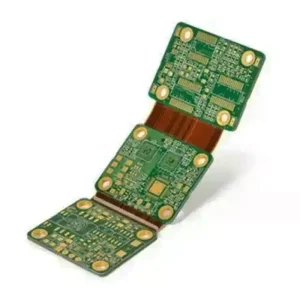
The Difference Between Rigid PCB and Flexible PCB
Rigid PCB, commonly referred to simply as PCBs, are what most people envision when thinking of circuit boards. These boards utilise conductive tracks and other components arranged upon a non-conductive
The Structure and Advantages of High-Conductivity Aluminium Substrate
Ultra-high thermal conductivity aluminium substrate is a novel circuit board that achieves exceptional thermal performance by replacing the resin insulating layer within existing metal aluminium-based circuit board structures with a

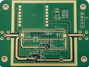
What is 5G millimetre wave and Interconnect Design Optimisation Strategies
What is 5G millimetre wave? 5G millimetre wave, also known as the millimetre wave band, refers to the spectrum segment with wavelengths between 1mm and 10mm, corresponding to frequencies ranging
The Effects and Optimisation of Thermal Stress in PCB substrate
Thermal stress refers to the mechanical stress arising from uneven thermal expansion or contraction within materials during temperature changes. Within the PCB substrate sector, thermal stress primarily originates from the