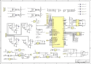
What is Schematic Diagram of PCB
In the modern electronics industry, schematic diagram of pcb are an indispensable and important part of the circuit design and manufacturing process. Whether you are a professional engineer or an
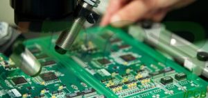
printed wiring board manufacturing process
Today we are going to explain the printed wiring board manufacturing process. If you are wondering, ” printed wiring board manufacturing process “, you have come to the right page.
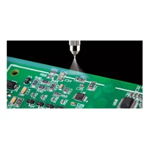
The Future of Conformal Coating in Electronics
In the production and maintenance of modern electronic equipment, the protection of electronic components has always been an important issue. In particular, in the face of various harsh environmental conditions,
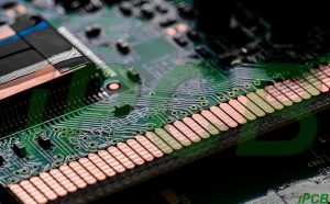
connector pcb edge
In the field of electronics, the connector pcb edge plays a vital role in establishing a reliable and secure connection with external devices. Whether you are working on a computer,
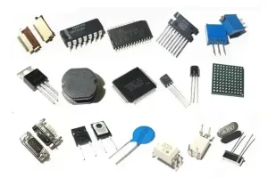
How to Identify Components on a Circuit Board
Circuit boards are an indispensable core part of modern electronic devices. They integrate various electronic components and realize various functions of the equipment through reasonable circuit design. However, for beginners,
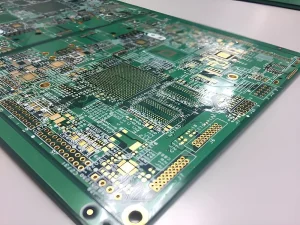
Comprehensive Analysis of Quick Turn Printed Circuit Boards
With the rapid development of the electronics industry, the demand for printed circuit boards is also growing. In this efficient and precise market environment, “fast-turn printed circuit boards” has become
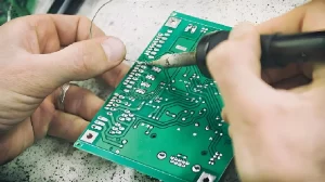
Process Analysis and Application Value of Solder Plugs
In the field of modern electronic manufacturing, with the widespread application of high-density, multi-layer PCBs, solder plugging technology has become one of the important processes to improve the performance and
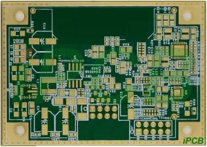
automotive radar antenna
One day in the future, self-driving vehicles may be safer than the motor vehicles driven by drivers today. But before drivers start to let go of the steering wheel, some
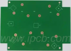
Copper oxydation pcb no solder mask
Copper oxydation pcb no solder mask is a special type of printed circuit board that protects the copper conductors by forming a stable copper oxide film instead of a solder
Tin plating technology for circuit board
What is tin plating?Tin plating is the application of a layer of tin to a copper foil. In the circuit board manufacturing process, the surface of the copper foil is
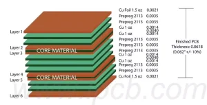
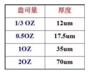
Thickness of pcb copper foil
In PCB (Printed Circuit Board) manufacturing, an ounce (OZ) is essentially a unit of weight, which converts to grams (g) roughly as follows: 1 OZ equals approximately 28.35 g. The
Remove solder from pcb to quality assurance
Solder flux residue is generally defined as the residual material left on the surface of a circuit board or other workpiece during a soldering operation or electronics manufacturing process due
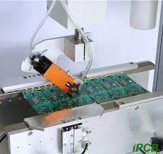
Can I cut PCB with scissors?
Can I cut PCB with scissors? Why do I need to cut PCBs?Cutting PCBs is an important process for customizing and optimizing electronic projects. There are several reasons for cutting
What is industry standard PCB thickness?
What is industry standard PCB thickness?The standard PCB thickness for 2 layers is 1.6mm.Depending on the specific requirements of the design, measurements other than the standard measurements are used in

How to check light emitting diode with multimeter
An LED (light emitting diode) is a semiconductor diode,specifically a p-n junction, that emits light when a positive current flows from the anode (labelled ‘+’, i.e., positive) to the cathode
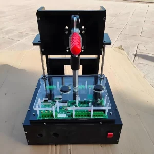
The value and realization of custom test fixtures
With the rapid development of electronic technology, more and more industries have continuously increased their requirements for product quality, especially in the production process of electronic products. How to test
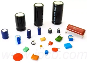
Overview of common components on a PCBA
PCBA processing is the core process of circuit board manufacturing, covering the two main aspects of PCB manufacturing and SMT placement processing, in which the addition of electronic devices is
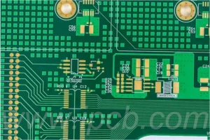
Functions of a normal keyboard PCB
A normal keyboard PCB, also known as a printed circuit board (PCB), is an essential component of the keyboard’s internal structure. It plays the role of receiving the user’s instructions
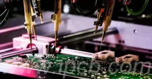
Flying probe test for PCB measurement
Flying probe testing is a method of testing electronic circuits, primarily for testing printed circuit boards (PCBs). It utilizes a system of movable probes that actually “fly” across the board,
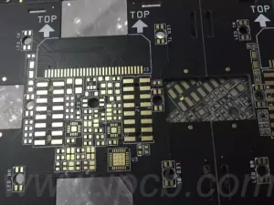
PCB solder mask selection and application
Solder mask is a key technology in the manufacture of PCBs (Printed Circuit Boards), designed to protect the metal components of the board from oxidation and to avoid the formation

pcb board stackup
Generally speaking, when designing ordinary single-sided and double-sided boards, there is no need to consider the pcb board stack up problem. Usually, copper clad boards with copper thickness and board
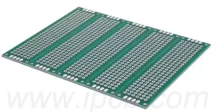
Glass pcb and TGV carrier board manufacturing process
Glass pcb and their derivatives, glass through hole (TGV) carrier board,has become indispensable core components for various high-tech electronic products. They are not only widely used in liquid crystal display
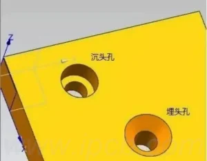
Countersunk hole in PCB applications and manufacturing
A countersunk hole is a semi-penetrating hole in a circuit board made with a flat head drill or gong cutter, characterised by the fact that the hole does not run
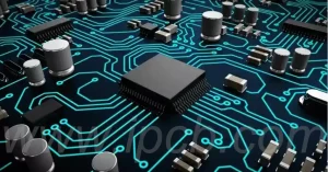
PCBA IC Pin Moulding Process
PCBA (Printed Circuit Board Assembly) integrated circuit lead forming process is an important technology in modern electronics manufacturing, which involves adapting the pins of integrated circuits to the specific shape