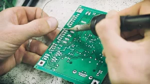
Double Sided PCB Soldering Tips
PCB soldering precautions1.EDA365 electronic community suggests that the first task after obtaining the PCB bare board is to carry out visual inspection to confirm that there are no short circuits,
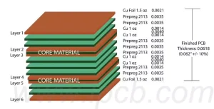
Double sided pcb board manufacturing process challenges
The production process for double sided pcb board consists of several stages, each of which may face a number of technical challenges.The following are some of the major challenges: Design
How to Wire PCB mono input jack
In the design of modern electronic products, audio input and output are very important, especially in the design of audio equipment. As part of the audio equipment, the mono input
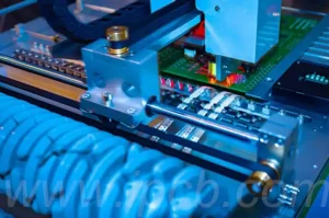
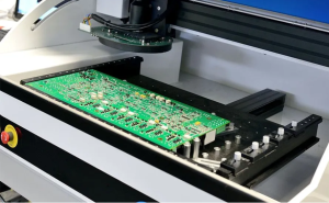
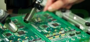
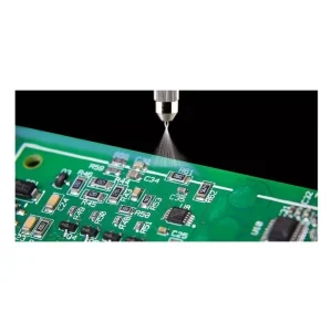
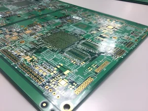
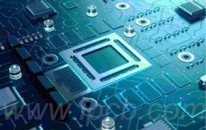
PCBA SMD preparation and processing considerations
PCBA chip processing is one of the core links in the manufacturing process of electronic products, which includes a number of stages from circuit design to product moulding. Each stage
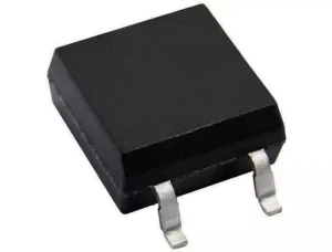
What does ctr stand for on a pcb
What does ctr stand for on a pcb? The current transfer ratio (CTR) is a critical parameter in electronic design and component selection, especially in optocouplers, where CTR not only
Can you use ac in a pcb
Can you use ac in a pcb? Circuit boards can use either AC or DC as a power source, depending on the design and purpose of the board. Some circuit
PCB pad types and their design guidelines
In PCB design,pads as a bridge connecting components and circuit boards, its type and design standards are critical. Different types of pcb pads are suitable for different components and application
Is RF Assembly High Frequency or Low Frequency?
In modern communications and electronic technology, RF components play a vital role. However, many people still have doubts about the characteristics and operating frequency of RF components: Is RF assembly
ate in pcba testing
Ate in pcba testing means testing the electrical conductivity and input-output values of the PCBA circuit board with mounted electronic components. In the design of the PCB circuit board, there
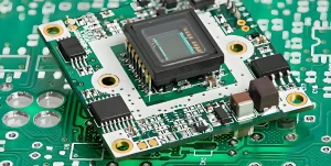
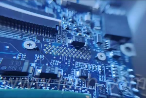
Key Insights into Circuit Card Assembly
In modern electronic devices, circuit card assembly are a core part that carries signal transmission, data processing and various control functions. Whether in smartphones, computers, or industrial automation equipment, circuit
Introduction of PCB radar
PCB radar is a circuit board specially designed for use in radar systems to connect and support various electronic components and devices in the radar system. It plays a key
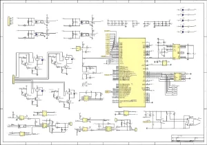
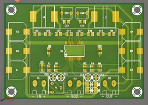
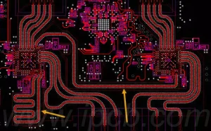
What is Schematic Diagram of PCB
In the modern electronics industry, schematic diagram of pcb are an indispensable and important part of the circuit design and manufacturing process. Whether you are a professional engineer or an
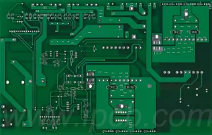
printed wiring board manufacturing process
Today we are going to explain the printed wiring board manufacturing process. If you are wondering, ” printed wiring board manufacturing process “, you have come to the right page.
The Future of Conformal Coating in Electronics
In the production and maintenance of modern electronic equipment, the protection of electronic components has always been an important issue. In particular, in the face of various harsh environmental conditions,
connector pcb edge
In the field of electronics, the connector pcb edge plays a vital role in establishing a reliable and secure connection with external devices. Whether you are working on a computer,
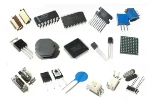
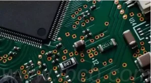
How to Identify Components on a Circuit Board
Circuit boards are an indispensable core part of modern electronic devices. They integrate various electronic components and realize various functions of the equipment through reasonable circuit design. However, for beginners,
Comprehensive Analysis of Quick Turn Printed Circuit Boards
With the rapid development of the electronics industry, the demand for printed circuit boards is also growing. In this efficient and precise market environment, “fast-turn printed circuit boards” has become
Process Analysis and Application Value of Solder Plugs
In the field of modern electronic manufacturing, with the widespread application of high-density, multi-layer PCBs, solder plugging technology has become one of the important processes to improve the performance and
automotive radar antenna
One day in the future, self-driving vehicles may be safer than the motor vehicles driven by drivers today. But before drivers start to let go of the steering wheel, some
Copper oxydation pcb no solder mask
Copper oxydation pcb no solder mask is a special type of printed circuit board that protects the copper conductors by forming a stable copper oxide film instead of a solder
Tin plating technology for circuit board
What is tin plating?Tin plating is the application of a layer of tin to a copper foil. In the circuit board manufacturing process, the surface of the copper foil is
Thickness of pcb copper foil
In PCB (Printed Circuit Board) manufacturing, an ounce (OZ) is essentially a unit of weight, which converts to grams (g) roughly as follows: 1 OZ equals approximately 28.35 g. The
Remove solder from pcb to quality assurance
Solder flux residue is generally defined as the residual material left on the surface of a circuit board or other workpiece during a soldering operation or electronics manufacturing process due
Can I cut PCB with scissors?
Can I cut PCB with scissors? Why do I need to cut PCBs?Cutting PCBs is an important process for customizing and optimizing electronic projects. There are several reasons for cutting