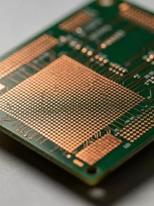
Causes and Solutions for Blackening of Gold Plating on PCB Boards
During the PCB manufacturing process, the darkening of the gold plating layer is a relatively common cosmetic defect. This not only affects the visual appearance of the product but may
Strategies for Preventing Delamination in High TG Laminates
High TG laminates refer to materials with a Tg value typically above 170°C; for example, common lead-free compatible laminates can have a Tg of around 185°C. Furthermore, the thermal decomposition
FR4 PCB baking process
In the electronic assembly process, the baking of FR4 PCBs may seem unremarkable, but it is in fact a critical step that determines the quality of the solder joints. Its
Differences between rolled copper and electrolytic copper in high frequency PCBs
Rolled copper and electrolytic copper are the two main types of copper foil used in high frequency PCBs for lamination with PTFE boards. Due to differences in their manufacturing processes,
Thermal conductivity of PTFE PCBs
Unlike standard PCB substrates, the thermal conductivity of PTFE PCBs is not determined solely by the substrate itself, but rather by the combined effects of substrate properties, filler modification, manufacturing
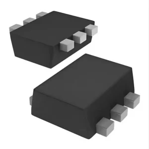
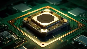
Types, Processes and Advantages of Ball Grid Arrays (BGAs)
What is a BGA? When dealing with high-density integrated circuits (ICs) – such as microprocessors or complex ASICs – you are likely to encounter ball grid arrays (BGAs). Unlike traditional
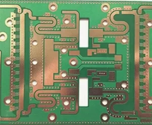
Multilayer RF PCB Design
Unlike standard PCBs, the core of multilayer RF PCB design lies in balancing signal integrity with manufacturability. High-frequency signals are prone to attenuation, reflection and crosstalk during transmission, and the
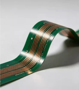
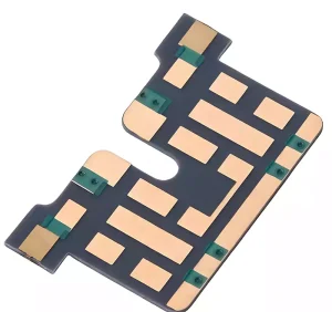
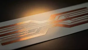
FPC laminate design
Flexible printed circuit boards (FPCs), with their inherent properties of being bendable, foldable, lightweight, and compact, are ideally suited to the requirements of tight spaces and complex structural assemblies in
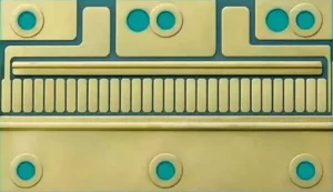
Differences in the stacking structures of through hole board and HDI board
The stack up design of a PCB (printed circuit board) directly determines its electrical performance, mechanical reliability, manufacturability and cost. Among these, Through Hole Board and HDI boards are the
An Analysis of High-Density Interconnect (HDI PCB) Technology
HDI PCB(High Density Interconnect) is a core PCB manufacturing process designed for high-density wiring, characterised primarily by the use of micro-blind vias and buried blind vias to achieve efficient interconnection
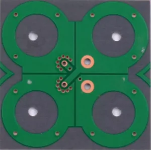
Understanding Substrate Diode and Packaging Substrate
In the efficiency race of power electronics systems, engineers often focus on “front-end parameters” such as the on-resistance, gate charge, and reverse recovery charge of switching devices. However, a deeper,
PCB Circuit Formation Processes: Tenting, SAP and mSAP
In the field of PCB manufacturing, the circuit patterning process is a critical factor in determining the performance and quality of the PCB. Among these, Tenting (subtractive process), SAP (semi-additive
High frequency PCB design for military radar
High frequency PCBs for military radar serve as the core hardware platform within radar systems, undertaking critical tasks such as signal transmission, power amplification and processing; their performance directly determines
The Application and Optimisation of AOI Technology in PCB Manufacturing
Automated Optical Inspection (AOI) is a core quality inspection technology in the PCB manufacturing sector. It relies on machine vision and image recognition technologies, combining lighting systems, high-definition camera systems
Tips for designing thick copper PCBs
The design of thick copper PCBs differs significantly from that of conventional thin copper PCBs. The core challenge lies in ‘balancing high current-carrying capacity, efficient heat dissipation and manufacturing feasibility’—line
Causes and Control of Undercutting in the PCB Etching Process
Underetching of PCB circuit traces primarily occurs during the etching process. Any deviation in the concentration, temperature, spray pressure or etching time of the etching solution will significantly increase the
Comparison of Ceramic PCB Manufacturing Processes: Subtractive and Additive Methods
Every improvement in the precision of flexible circuit formation drives the expansion of ceramic pcb into high-end applications such as 5G communications, medical electronics and aerospace. As the two core
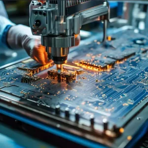
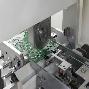
An Analysis of the SMT Assembly Process
Surface Mount Technology Assembly (SMT Assembly) is an electronic assembly technique in which leadless or short-lead surface-mount devices (SMDs) are directly soldered onto the surface of a printed circuit board
High-frequency low-loss FPC material
High-frequency, low-loss FPCs (flexible printed circuit boards) are the key medium for signal transmission in 5G communication equipment; their material properties directly determine the transmission speed, stability and coverage of
A Detailed Guide to Metal Core PCBs(MCPCBs)
Metal Core PCB (MCPCBs), also known as Insulated Metal Substrate (IMS) PCBs or thermal PCBs, are a type of printed circuit board that uses a metal plate as the substrate
Ceramic circuit boards in extreme-duty military sensors
Ceramic circuit boards offer unique advantages in terms of wide temperature ranges, high thermal conductivity, high-frequency stability and resistance to harsh environments, enabling them to meet the stringent requirements of
Key Characteristics and Applications of High Frequency PCB Materials
With the trend towards higher frequencies, miniaturisation and higher performance in electronic devices, high frequency PCBs (printed circuit boards) are now widely used in fields such as 5G communications, satellite
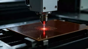
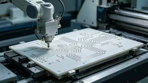
The role of PCB cutting machines in the electronics industry
Industry Challenges, Evolution, and the Historical Framework of PCB Cutting machines Technology About pcb cutting machines, In an era where electronic product iteration cycles are measured in months, the PCB,
The impact of PCB ink on PCB performance
In the PCB manufacturing process, although pcb inks are classified as auxiliary materials, they play an indispensable role in PCB circuit boards. Different types of ink not only determine the